
Flyback and forward converters can look deceptively similar in an isolated switching power supply circuit. Both use a high-frequency magnetic component to provide isolation and voltage scaling. Inside the power stage, however, they move and store energy in different places. That difference shapes the transformer, semiconductor stress, control loop, output ripple, thermal behavior, and ultimately the applications each topology handles well.
For most design teams, the useful question is not which topology is “better.” It is which one reaches the required electrical performance with acceptable component count, engineering effort, and production risk. A modest auxiliary rail may favor a flyback even when its peak currents are higher. A higher-current, tightly regulated output may justify the extra rectifier and output inductor of a forward converter.
The design decision starts with energy transfer
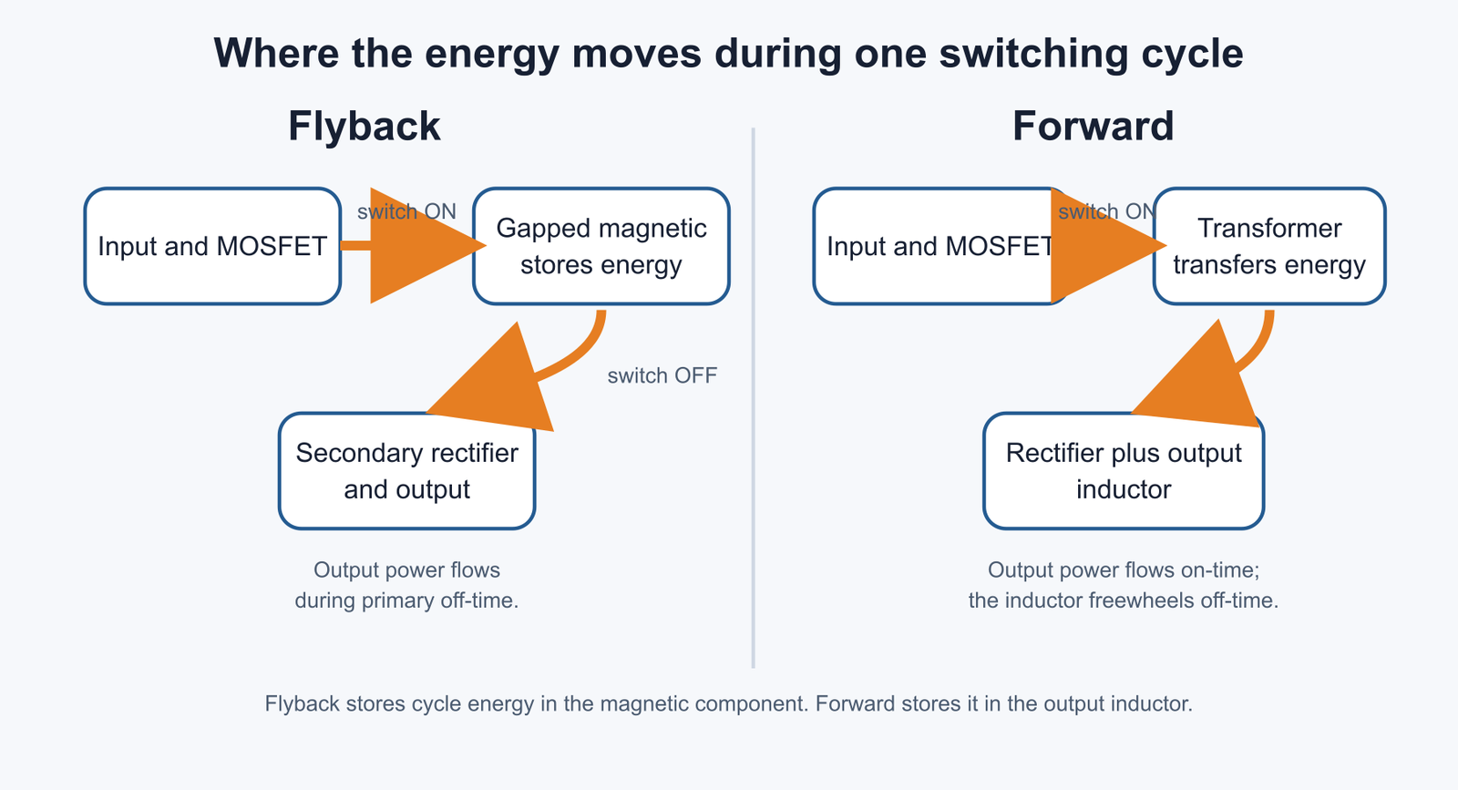
In a flyback converter, the magnetic component behaves as a coupled inductor. While the primary switch is on, primary current ramps up and energy accumulates in the gapped core. The secondary rectifier is reverse-biased during this interval. When the switch turns off, the winding polarities reverse and stored energy flows to the output.
A forward converter transfers energy to the secondary while the primary switch is on. Its transformer is intended mainly for isolation and voltage conversion, not for storing the cycle’s useful output energy. An output inductor receives energy during the on-time and freewheels through a second rectifier during the off-time. The transformer magnetizing flux must also be reset before the next cycle.
| Design dimension | Flyback converter | Forward converter |
|---|---|---|
| Magnetic component | Gapped coupled inductor stores energy | Transformer transfers energy; little or no intentional gap |
| Output power interval | Mainly during primary off-time | During primary on-time; output inductor freewheels off-time |
| Secondary power stage | Rectifier and output capacitor | Main rectifier, freewheel path, output inductor, output capacitor |
| Main magnetic risk | Saturation, leakage energy, winding capacitance | Incomplete core reset, flux walking, leakage overshoot |
| Control behavior | CCM has a right-half-plane zero; mode changes matter | Buck-derived power stage; usually easier to compensate |
| Natural advantage | Low parts count and easy isolated multi-output implementation | Lower output-current ripple and better transformer utilization |
Flyback switching power supply design points
Choose the reflected voltage before choosing the MOSFET
The turns ratio fixes the output voltage reflected to the primary. For an ideal CCM flyback,
(VOUT + VF) / VIN = (NS / NP) × D / (1 − D)
The drain voltage after turn-off is approximately the maximum input bus voltage plus the reflected output voltage, followed by a leakage-inductance spike. A high reflected voltage reduces secondary diode stress and can shorten demagnetization time, but it raises MOSFET voltage stress. A low reflected voltage does the opposite. The practical design variable is therefore reflected voltage, not turns ratio in isolation.
For an offline AC-DC switching power supply, select the MOSFET only after estimating the worst-case rectified input, clamp voltage, measured leakage overshoot, surge requirements, and the company’s derating rule. “Use a 650 V MOSFET” is not a design method; it is only a common outcome for some universal-input products.
Set magnetizing inductance from current and energy targets
During the on-time, primary current ripple is approximately:
ΔIP = VIN × D / (LP × fSW)
In DCM or boundary operation, the energy processed per cycle is closely related to ½ × LP × IPK². In CCM, magnetizing inductance also sets ripple, RMS current, and the location of dynamic constraints. A larger inductance reduces ripple but may require a smaller gap, more turns, or a larger core to preserve saturation margin. A smaller inductance raises peak and RMS currents.
The core and gap must be checked at the highest relevant temperature and worst-case current limit, including tolerances. Gap length alone is not a transferable rule. A 1 mm gap may be excessive in one core and inadequate in another; the required gap follows the target inductance, turns count, effective core area, and stored energy.
Treat the clamp as part of the power stage
Leakage inductance cannot deliver all of its energy to the secondary. When the primary switch turns off, that energy produces a drain-voltage spike. An RCD clamp is inexpensive and forgiving, but it dissipates energy. A TVS or Zener-assisted clamp offers tighter voltage limiting in suitable power ranges. Active-clamp flyback recycles part of the leakage energy and can enable softer switching, at the cost of another switch, more control complexity, and more demanding timing.
Clamp loss should be estimated, then verified with the production-intent transformer. Winding construction changes leakage inductance, capacitance, ringing, and common-mode EMI. A clamp calculated from a prototype transformer may not remain correct after the winding house changes insulation tape, layer order, or bobbin fill.
Do not reduce DCM and CCM to a single efficiency claim
DCM lets the secondary current return to zero every cycle. It can simplify rectifier commutation and works well in low-power designs, but peak current is higher. CCM lowers peak-to-average current at higher load, while introducing a right-half-plane zero in the control-to-output response. That zero limits achievable crossover frequency and makes compensation more sensitive.
Light-load overvoltage is not an unavoidable law of a regulated DCM flyback. A competent controller reduces delivered energy through pulse-frequency modulation, burst operation, or skipped cycles. The difficult cases are often auxiliary outputs, poor minimum-load assumptions, transformer-coupling error, or feedback that regulates only one winding. Multi-output cross-regulation therefore needs load-matrix testing, not just a nominal full-load check.
Verify the secondary side at the actual current waveform
The rectifier sees a pulsed current rather than a smooth DC current. Its RMS current, peak current, reverse voltage, junction temperature, and reverse-recovery behavior must be calculated for the selected operating mode. Low-voltage, high-current outputs often benefit from synchronous rectification, but controller timing must prevent reverse current and cross-conduction.
The output capacitor supplies the load during the primary on-time and absorbs pulsed secondary current after turn-off. Capacitance, ESR, ripple-current rating, temperature, and lifetime all matter. A capacitance-only selection commonly passes the voltage-ripple target on paper and fails thermal or lifetime testing.

Forward converter design points that set reliability
Core reset is a first-order constraint
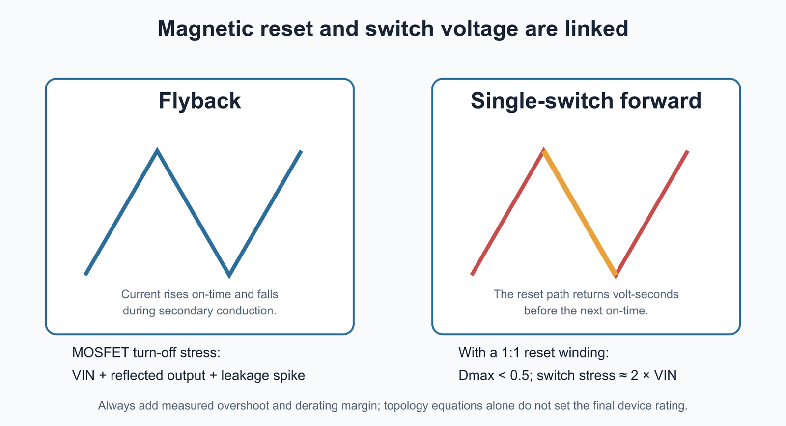
The forward transformer receives positive volt-seconds while the main switch is on. It needs a defined path for negative volt-seconds during the off-time. A reset winding, RCD clamp, active clamp, or two-switch arrangement can provide that path.
With a conventional reset winding, the maximum duty cycle is constrained by the primary-to-reset turns ratio. When the reset and primary turns are equal, the theoretical duty-cycle ceiling is 0.5; practical control limits must be lower to allow tolerances and complete reset. The main switch in this arrangement ideally sees about twice the input bus voltage before leakage overshoot. This is an important correction to the common assumption that a single-switch forward MOSFET only blocks the input voltage.
In a two-switch forward converter, two primary switches and clamp diodes return magnetizing energy to the input. Each switch is ideally clamped near the input voltage, which eases voltage stress and makes the topology attractive at higher input voltage. It does not eliminate the need to verify dead time, leakage ringing, driver behavior, and simultaneous switching.
Size the switch mode power supply transformer by volt-seconds and temperature
For a rectangular applied voltage, a useful first check is:
ΔB ≈ VIN × D / (NP × AE × fSW)
The permitted flux swing depends on core material, frequency, waveform, loss target, and hot operating temperature. Using saturation flux density as the normal design point leaves no practical margin. Core-loss data and thermal rise usually impose a lower working flux density than the material’s saturation limit.
Because the forward transformer does not intentionally store the output energy, it normally has no deliberate energy-storage gap. A small mechanical gap can exist in a real assembly, but adding a flyback-style gap increases magnetizing current and undermines the design.
Design the output stage as an isolated buck
Ignoring losses, the conversion ratio is:
VOUT ≈ VIN × (NS / NP) × D
The output inductor ripple can be estimated during the on-time from:
ΔIL ≈ [VIN × (NS / NP) − VOUT] × D / (LO × fSW)
The freewheel interval gives an equivalent check using VOUT and (1 − D). Design teams should calculate both and reconcile them at the steady-state operating point. Inductor saturation, copper loss, core loss, fringing, and hot inductance tolerance then determine the final part.
The main rectifier and freewheel rectifier carry different waveforms. Their average and RMS currents are not interchangeable, and their reverse-voltage stress depends on the secondary waveform and clamp behavior. Synchronous rectification can materially reduce conduction loss on low-voltage outputs, but it adds gate-drive and timing risk.
Layout must contain three high di/dt loops
The primary switch loop, secondary main-rectifier loop, and freewheel loop should each be compact. The clamp belongs physically close to the device and winding it protects. Keep noisy drain or rectifier nodes away from feedback, current-sense, and isolation components. Transformer interwinding capacitance and the Y-capacitor strategy also affect common-mode noise; shortening a loop does not, by itself, solve conducted or radiated EMI.
Where each topology fits
Power level is a useful screen, not a universal boundary. A conventional flyback switching power supply is common in low-power isolated AC-DC supplies and auxiliary rails. Well-executed CCM, quasi-resonant, active-clamp, or interleaved designs can extend it higher. Forward converters have historically covered moderate power where lower current ripple and better magnetic utilization justify more components. In a DC-DC switching power supply, the input range and output current can shift that crossover substantially. At still higher power or demanding switch mode power supply efficiency, LLC, half-bridge, phase-shifted full-bridge, and other architectures often deserve comparison.
| Application condition | Likely starting point | Why | What could change the decision |
|---|---|---|---|
| Low-cost isolated auxiliary supply | Flyback | Few power components; wide input and multiple outputs are practical | Tight cross-regulation or high standby-efficiency target |
| Adapter, appliance control, small industrial control rail | Flyback or quasi-resonant flyback | Mature controllers and compact magnetics | High continuous power, sealed enclosure, strict thermal limit |
| Multiple isolated outputs at modest total power | Flyback | Additional secondary windings need relatively little hardware | One output has high current or all rails need tight independent regulation |
| Moderate-power low-voltage high-current output | Two-switch or active-clamp forward | Lower output ripple and favorable switch stress | LLC may win if efficiency and power density dominate |
| PoE powered device or telecom DC-DC stage | Flyback at lower power; active-clamp forward at higher current | Both topologies have established controller ecosystems | Input range, hold-up, transient response, and isolation capacitance |
| Very high efficiency or several hundred watts and above | Compare resonant or bridge topologies | Switching and conduction losses can dominate | Cost, bidirectional operation, regulation range, and development schedule |
A design review checklist
| Review area | Flyback questions | Forward questions |
|---|---|---|
| Magnetics | Is the gap controlled? Are peak flux, copper loss, leakage, and capacitance acceptable hot? | Is reset complete at maximum duty cycle? Are flux swing, core loss, and magnetizing current acceptable hot? |
| Primary switch | Does rating cover maximum bus, reflected voltage, clamp level, overshoot, and surge derating? | Does rating match the reset method: about 2 × VIN for a 1:1 reset winding or about VIN per switch in a two-switch stage, plus overshoot? |
| Secondary | Are pulsed RMS current, reverse voltage, capacitor ripple current, and cross-regulation verified? | Are main and freewheel rectifier stresses calculated separately? Does the output inductor avoid saturation? |
| Control | Is the operating mode defined across line and load? Is crossover safely below the CCM right-half-plane zero? | Are duty-cycle limits coordinated with reset time? Is current-mode slope compensation needed? |
| Protection | Do OCP, OVP, short-circuit, startup, brownout, and open-feedback tests behave safely? | Do reset failure, driver fault, short-circuit, and output-inductor saturation tests behave safely? |
| Production | Have transformer tolerances and clamp loss been tested across lots? | Have reset winding polarity, switch timing, and output-inductor tolerance been error-proofed? |
Common mistakes that cost prototype cycles
A flyback often fails late because the design team optimizes the schematic but treats the transformer as a nominal inductance. Leakage, winding capacitance, hot saturation margin, and insulation construction are part of the circuit. Another recurring mistake is using average diode current to size a rectifier that carries high triangular peaks.
A forward converter can pass initial regulation tests while accumulating flux at one corner of the operating range. Duty-cycle limits, startup pulses, current-limit behavior, and reset timing all need oscilloscope verification. In two-switch designs, the gate-drive paths should be matched, but a universal sub-5 ns mismatch rule is not meaningful without the devices, switching speed, and driver architecture.
For either topology, measure switch voltage with a short ground spring or a properly connected differential probe. A long probe ground lead can create a ringing waveform that belongs to the measurement loop rather than the converter. Thermal testing should use the worst credible line, load, enclosure, and ambient combination after the unit reaches equilibrium.
Choosing with fewer assumptions
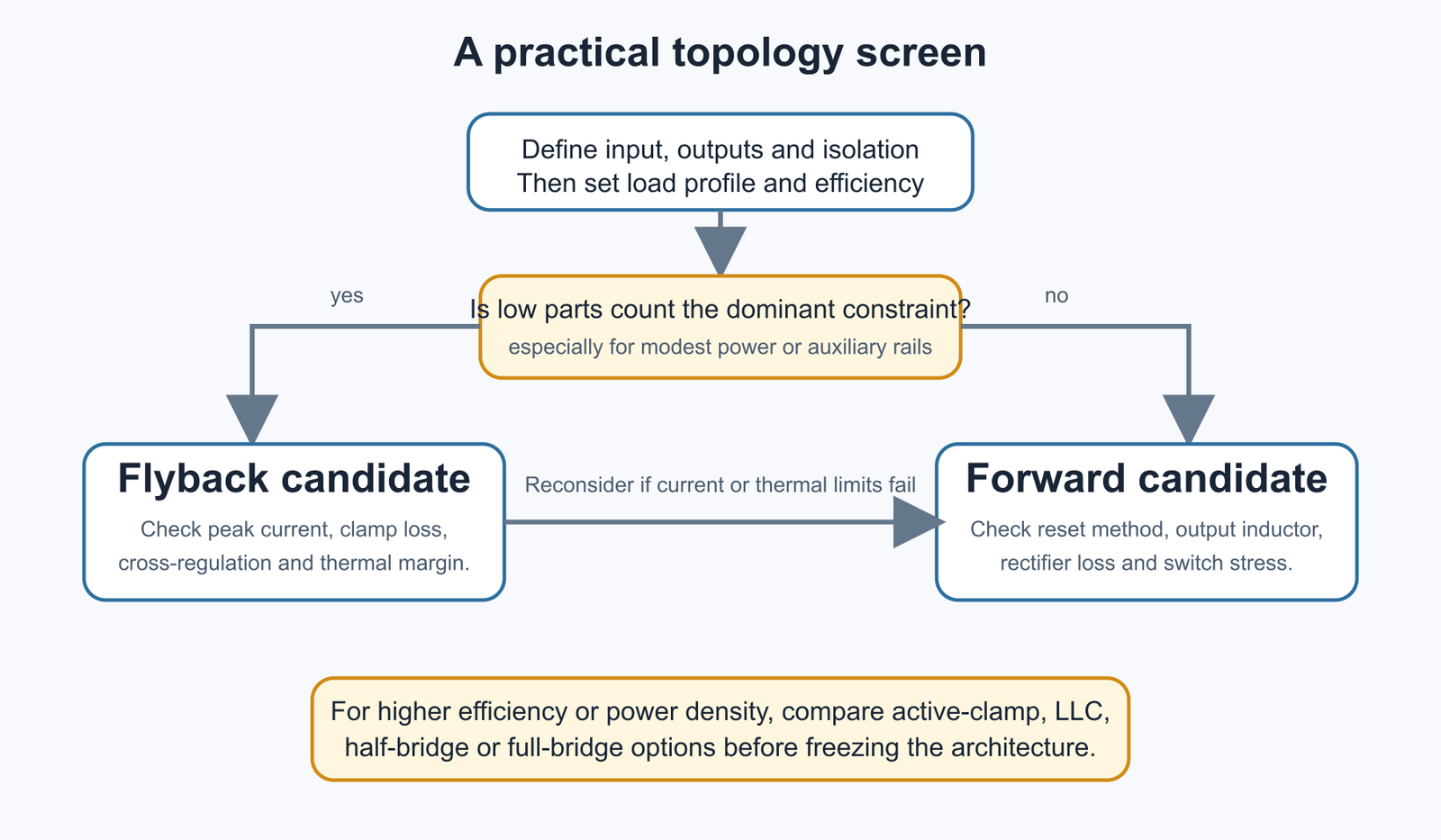
Choose a flyback when low component count, economical isolation, and multiple modest-power outputs matter more than peak current and cross-regulation. Choose a forward converter when output current, ripple, thermal efficiency, or transformer utilization justifies a more involved power stage and a deliberate reset system.
Do not freeze the topology from wattage alone. Establish the input range, output matrix, overload profile, hold-up requirement, isolation system, efficiency target, enclosure temperature, EMC limits, and cost ceiling. Then compare estimated loss and stress at the corners. This produces a more useful switch mode power supply design than selecting a familiar topology first and forcing the transformer and clamp to fit. SIPURUI can support industrial power-supply selection and customization when a project needs these constraints translated into a production-ready AC-DC or DC-DC specification.