
A MOSFET gate driver is small compared with the power stage, but it controls how the power stage behaves. Its job is not simply to make the MOSFET turn on and off. A good driver moves the required gate charge at a controlled rate, holds the device off during high dV/dt events, limits gate overshoot and ringing, and keeps the switching loop repeatable across temperature and production variation.
Those objectives apply to flyback converters, buck stages, LLC half bridges, synchronous rectifiers, motor drives, and other switched-power systems. The exact voltage and timing targets differ by device and topology, but the design method is the same: start from the MOSFET data, estimate the necessary source and sink current, build a low-inductance gate loop, and tune the final values from measured waveforms.
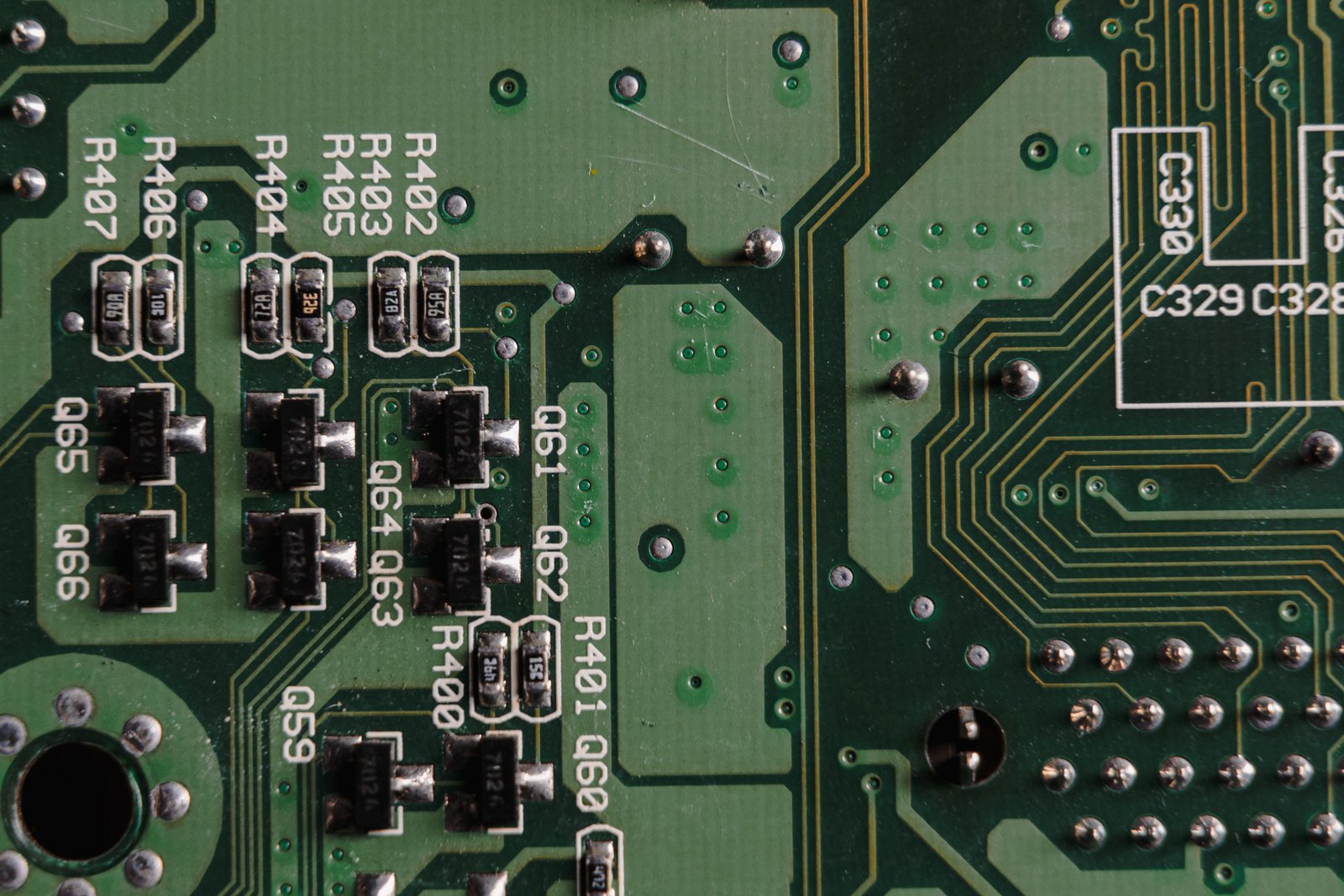
What the Gate Driver Must Control
The gate behaves mainly as a nonlinear capacitive load. During every switching cycle, the driver must supply and remove charge. The most important design outcomes are:
a transition fast enough to keep switching loss within the thermal budget;
a transition slow and well damped enough to control overshoot, ringing, and EMI;
adequate off-state immunity against Miller current and common-source inductance;
gate-source voltage that remains inside the device's absolute maximum ratings; and
reliable timing between switches in half-bridge and synchronous topologies.
There is no universally correct “fastest” gate drive. Faster edges can reduce overlap loss while increasing dV/dt, di/dt, drain overshoot, common-mode current, and susceptibility to false turn-on. The best setting is the fastest transition that still meets voltage-stress, EMI, thermal, and reliability limits.
Read the MOSFET Data Before Choosing the Driver
Gate-drive voltage is not the threshold voltage
The gate threshold voltage, VGS(th), is measured at a very small drain current. It does not tell you the voltage needed for low on-resistance. Use the RDS(on) test conditions and the gate-charge curve in the MOSFET datasheet.
Many conventional silicon power MOSFETs are characterized around 10 V. Logic-level parts may be fully specified at 4.5 V or lower. Some driver systems use 12 V, but the correct value is the voltage at which the chosen MOSFET is specified, with enough margin for supply tolerance and transient droop. Do not apply 15 V merely to make a standard silicon MOSFET switch harder: many devices have a ±20 V absolute maximum VGS rating, leaving little room for overshoot. SiC MOSFETs and GaN devices use different recommended voltage windows and must follow their own datasheets.
The normal off-state level for a silicon MOSFET is 0 V. A negative rail may be useful in a high-dV/dt bridge, but it is not automatically required. Negative bias must remain within the device's negative VGS rating and any lifetime guidance from the semiconductor supplier. An active Miller clamp or stronger local pull-down can sometimes provide the needed immunity without a negative rail.
Gate charge matters more than a single input-capacitance number
Input capacitance is useful for small-signal comparison, but gate charge is usually the better design quantity for switching. The total charge Qg includes the gate-source charge Qgs and gate-drain charge Qgd. Qgd is associated with the Miller plateau, where drain voltage changes while gate voltage remains nearly flat. Driver current during this interval has a strong influence on dV/dt and switching loss.
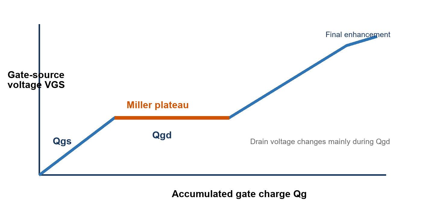
A first estimate of average driver supply current is:
IAVG ≈ Qg × fSW × N
where N is the number of MOSFETs being driven. This value helps size the bias supply, but it is not the required peak output current. A useful first estimate for transition current is:
IG ≈ QSW / tSW
Use the relevant charge interval, especially Qgd when estimating the drain-voltage transition. For example, moving 12 nC in 40 ns requires about 0.30 A at the gate. Real current is limited by the driver's output resistance, external resistor, MOSFET internal gate resistance, and interconnect impedance, so the selected driver needs margin beyond this simple quotient.
Source current and sink current may need different values
Turn-on current controls how quickly the device enters the Miller region and how aggressively drain current commutates. Turn-off current determines how quickly charge is removed and how firmly the gate is held below threshold. Many designs deliberately use a larger Rgon and a smaller Rgoff. This reduces turn-on di/dt while preserving a strong turn-off path.
Choosing the Gate Resistor
The external gate resistor works with the driver's output resistance, the MOSFET's internal gate resistance, and parasitic inductance. It sets current and provides damping; it should not be treated as an isolated component value.
| Change | Likely benefit | Likely penalty |
|---|---|---|
| Increase Rgon | Lower turn-on dV/dt and di/dt; less ringing and EMI | Higher turn-on switching loss; more heating |
| Decrease Rgon | Lower turn-on overlap loss | More overshoot, ringing, EMI, and possible false turn-on in the opposite switch |
| Decrease Rgoff | Stronger turn-off and better Miller immunity | Faster turn-off can increase drain overshoot |
| Increase Rgoff | Softer turn-off and potentially lower overshoot | Greater susceptibility to dV/dt-induced gate rise |
Values such as 5 Ω to 50 Ω are common starting points in lower-power silicon MOSFET converters, while high-current drivers may begin in the low single-digit ohm range. These are bench-start values, not design rules. Package type, Qgd, loop inductance, driver resistance, bus voltage, current, and snubber design can move the optimum far outside those ranges.
Avoid a zero-ohm default. With a strong driver and a low-inductance package, the resulting gate-loop LC network can ring hard enough to cross the threshold repeatedly or exceed the VGS rating. A small resistor close to the gate is cheap damping and also gives the engineer a controlled tuning point.
Selecting the Driver Circuit
Direct drive from the controller
Direct drive is suitable when the PWM controller's source and sink ratings are adequate for the MOSFET charge and target transition time. Check the output-current rating at the relevant voltage, not only a headline peak value. Confirm output resistance, propagation delay, UVLO behavior, and power dissipation. Place the gate resistor at the MOSFET gate rather than beside the controller if ringing control is the priority.
External push-pull or totem-pole buffer
A discrete NPN/PNP buffer or dedicated non-isolated gate driver provides more source and sink current and prevents the controller output from carrying the full gate pulse. It is useful with large MOSFETs or several parallel devices. The buffer needs local decoupling and a short return path. Its storage time and cross-conduction behavior also need review; a fast MOSFET driver IC is often more predictable than a casual discrete stage.
Isolated driver or gate-drive transformer
Isolation is used when the switch source moves with a high-voltage node or when reinforced isolation is required. An isolated driver IC provides defined UVLO, propagation delay, common-mode transient immunity, and often Miller clamping or desaturation functions. A gate-drive transformer can be economical for AC-coupled, balanced waveforms, but duty-cycle imbalance, magnetizing current, leakage inductance, startup state, and DC restoration must be managed. A transformer does not inherently guarantee a safe negative off voltage.
Bootstrap high-side driver
A bootstrap supply is common for the high-side N-channel device in buck and half-bridge stages. The bootstrap capacitor must deliver gate charge, driver quiescent current, leakage, and other dynamic charge without allowing the floating supply to fall below the driver's UVLO or the MOSFET's required gate voltage.
A practical sizing relationship is:
CBOOT ≥ QTOT / ΔVBOOT
where QTOT includes MOSFET gate charge plus the driver's high-side consumption and leakage over the maximum on-time. Apply a design margin and account for capacitor bias derating. Also verify that the low-side interval is long enough to recharge the capacitor. A bootstrap circuit cannot maintain arbitrary 100% high-side duty cycle without an auxiliary charging method.
Preventing Miller Turn-On
When the opposite switch changes the half-bridge node quickly, current flows through the off-state MOSFET's Cgd. The approximate injected current is:
IMILLER = Cgd × dVDS/dt
That current develops voltage across the gate's turn-off impedance. If the local VGS rises above threshold, the MOSFET can turn on briefly and create shoot-through. The risk increases with high dV/dt, high turn-off resistance, long gate wiring, common-source inductance, and a low threshold at high temperature.
Useful countermeasures are applied in layers:
Minimize the gate-to-source turn-off loop and use a Kelvin-source connection when available.
Provide enough sink current and select a sensible Rgoff.
Add an active Miller clamp close to the MOSFET if the driver supports it.
Use negative off bias only when justified and within the device's allowed voltage window.
Adjust the opposite device's turn-on edge if the switching-node dV/dt is unnecessarily high.
PCB Layout Requirements
The critical gate loop is driver output → gate resistor → MOSFET gate → MOSFET source/Kelvin source → driver ground. Its area should be small, and the forward and return traces should be close together. Wide copper alone is not enough if the return path takes a long detour.
Common-source inductance is especially damaging because the power current and gate return share impedance. During a rapid drain-current transition, the voltage across this inductance subtracts from or adds to the effective VGS. The result can be slower switching, ringing, or false turn-on. Packages with a Kelvin-source pin make it possible to separate the drive return from the high-current source path.
Place the driver decoupling capacitor directly across the driver's supply and ground pins. A 100 nF ceramic is a common high-frequency element, usually accompanied by a larger local capacitor selected for the pulsed gate-charge demand. Keep the gate trace away from the drain or switch-node copper. For isolated drivers, also respect creepage, clearance, and the isolation barrier's common-mode current path.
Protection, Dead Time, and Decoupling
A gate-source Zener or suitable TVS can limit positive gate overshoot, but it must have low inductance and a voltage that does not conduct heavily during the intended drive level. Confirm both positive and negative transient behavior. The clamp is backup protection, not a substitute for a stable loop.
In a half bridge or synchronous converter, dead time prevents simultaneous conduction. Too little dead time risks shoot-through. Too much dead time forces current through a body diode or third-quadrant channel, increasing loss and sometimes reverse-recovery stress. Set an initial value from worst-case propagation delays and switching times, then optimize on hardware across input voltage, current, temperature, and component tolerance. Qrr is relevant for silicon body-diode commutation, but it is not the only variable.
Driver-supply quality also deserves attention. A drooping VCC lengthens the Miller plateau and raises conduction loss; ringing on VCC can trip UVLO or overstress the driver. Measure the supply at the driver pins with the same care used for VGS.
A Practical Design Workflow
| Step | Design action | Evidence to keep |
|---|---|---|
| 1 | Record VGS ratings, recommended drive voltage, Qg, Qgd, internal Rg, RDS(on) conditions, and package/Kelvin options | Datasheet table and gate-charge graph |
| 2 | Choose target turn-on and turn-off times from loss, overshoot, and EMI goals | Loss estimate and topology constraints |
| 3 | Estimate average bias current and peak gate current | Qg × fSW and Q/t calculations |
| 4 | Select the driver topology and voltage rails | Source/sink rating, UVLO, isolation, CMTI, delay |
| 5 | Choose initial Rgon and Rgoff; size bootstrap and local decoupling | Calculation sheet and initial BOM |
| 6 | Route the compact gate loop and Kelvin return; separate it from the switch node | PCB review screenshot |
| 7 | Add gate clamp, Miller clamp, or negative bias only where the risk analysis supports it | Stress and false-turn-on margin |
| 8 | Measure VGS, VDS, drain current, driver VCC, and thermal behavior | Saved waveforms at operating corners |
Waveform Troubleshooting
| Symptom | Likely gate-drive cause | First checks and corrective actions |
|---|---|---|
| High-frequency VGS ringing | Gate-loop inductance is high; Rg is too small; probe loop is long | Use a ground spring or differential probe; shorten the loop; increase damping resistance |
| Random false turn-on or bridge failure | Miller injection, weak pull-down, common-source inductance, or poor dead time | Measure local VGS; reduce Rgoff; add Miller clamp; use Kelvin source; review complementary timing |
| MOSFET runs hot | Transitions are slow, drive voltage is low, or dead time creates diode conduction | Check the Miller interval, VCC droop, gate current, and switching energy |
| Miller plateau is unusually long | Insufficient driver current, excessive series resistance, VCC sag, or larger-than-assumed Qgd | Measure driver pin voltage and gate current; review Qgd at actual VDS and ID |
| Gate voltage overshoots its rating | Loop inductance and aggressive source/sink current; poorly placed clamp | Move the resistor/clamp to the gate; tune Rg; reduce loop area |
| VGS trace changes when the probe moves | Measurement inductance is dominating the result | Use a short spring ground or isolated differential probe connected directly across gate and source |
Do not diagnose gate ringing with a standard oscilloscope probe's long ground lead. That lead adds inductance and can create a waveform that does not exist at the device. For a ground-referenced low-side MOSFET, use the probe's ground spring and connect directly between gate and source. For a floating high-side device, use a properly rated differential probe with adequate common-mode rejection and voltage category.
Final Design Review Checklist
Before releasing the board, confirm that the selected gate voltage is supported by the MOSFET's RDS(on) data and remains inside both positive and negative limits. Verify driver source and sink current, UVLO, propagation delay, isolation rating where applicable, bootstrap recharge conditions, and local decoupling. Review the layout as a current-loop drawing rather than a list of nets. Finally, reserve accessible test points for gate-source measurement without adding a large measurement loop.
The gate driver should be treated as part of the power stage, not as a logic afterthought. A sound calculation narrows the search, but measured switching energy, overshoot, EMI, and temperature determine the final resistor and timing values. SIPURUI can support power-supply projects that need coordinated component selection, PCB layout review, and production-oriented validation rather than an isolated schematic check.