
A field reference for topology selection, component design, PCB layout, loop stability, EMC, and failure analysis
Switch-mode power supplies rarely fail because an engineer has forgotten what a buck converter does. They fail at the boundaries: a MOSFET selected from headline ratings, a current loop that grew during layout, a ripple measurement corrupted by the probe, or a compensation network tested at only one operating point.
This guide collects 34 questions that appear in design reviews, laboratory debugging, supplier discussions, and engineering interviews. The answers are intentionally practical. Numerical rules are treated as starting points, not universal limits, because topology, controller architecture, input range, output power, thermal design, safety class, and applicable EMC standard all change the result.
Fundamentals and operating modes
1. What is the core difference between a switching supply and a linear supply?
A linear regulator keeps its pass device in the active region and dissipates the unwanted voltage as heat. It can provide low output noise and simple control, but efficiency falls roughly with the ratio of output voltage to input voltage. A switching converter repeatedly turns semiconductor devices on and off, transfers energy through inductors or transformers, and filters the resulting waveform. That raises efficiency and power density, at the cost of switching ripple, fast-edge noise, and a more demanding layout.
The two are often combined. A switcher performs the efficient bulk conversion, followed by an LDO where a low-noise analog rail needs additional cleanup.
2. Why are “switching power supply” and “power switch” not interchangeable?
A switching power supply converts and regulates electrical energy. A power switch simply connects, disconnects, or routes power. A load switch, relay, or MOSFET high-side switch may include current limiting or protection, but it does not automatically provide regulated voltage conversion.
3. What do CCM and DCM mean?
In continuous conduction mode (CCM), the relevant inductor or transformer winding current does not return to zero during a switching period. CCM usually reduces peak and RMS current for a given power level, but some topologies acquire more difficult control dynamics. In discontinuous conduction mode (DCM), current falls to zero before the next cycle. DCM can simplify rectifier commutation and remove the right-half-plane zero from a flyback power stage, but it usually increases peak current, RMS loss, ripple, and EMI stress.
Light-load behavior deserves separate attention. Many controllers enter pulse skipping, burst mode, or another discontinuous operating scheme that is not identical to a power stage designed for DCM at rated load.
4. Where does the lost power go?
Loss is distributed across the circuit. MOSFETs incur conduction, switching, output-capacitance, body-diode, and gate-drive loss. Rectifiers contribute forward-drop and reverse-recovery loss. Magnetics add winding resistance, skin and proximity effects, core loss, gap fringing, and leakage-related dissipation. Capacitors dissipate ripple current through ESR. Current-sense elements, snubbers, clamp networks, controller bias supplies, optocouplers, and bleeders also consume power.
A useful loss budget is calculated at low line, nominal line, and high line, then checked at light and full load. The dominant mechanism often changes with the operating point.
5. What are ZVS and ZCS?
Zero-voltage switching (ZVS) commutates a device when its voltage is near zero. Zero-current switching (ZCS) commutates when current is near zero. Both reduce switching overlap loss and can reduce noise, but the resonant current needed to create the condition has its own conduction cost. LLC converters and phase-shifted full bridges use soft switching effectively at higher power, yet the soft-switching range still depends on load, dead time, magnetizing current, and parasitics.
Topology selection
6. When should I choose buck, boost, flyback, or LLC?
Topology should follow the electrical boundaries, not a remembered wattage chart.
| Topology | Conversion role | Strengths | Main cautions | Typical use |
|---|---|---|---|---|
| Buck | Step-down, non-isolated | Simple, efficient, low output ripple | Input hot loop and switch-node layout | Point-of-load rails, industrial DC/DC |
| Boost | Step-up, non-isolated | Efficient voltage lift | Output is not inherently disconnected; CCM has an RHP zero | Battery boost, PFC preregulators, LED strings |
| Flyback | Isolated step-up or step-down | Few parts, multiple outputs, wide input range | Pulsed currents, leakage spike, transformer design, control bandwidth | Auxiliary rails, adapters, industrial low-to-moderate power AC/DC |
| Forward | Isolated step-down | Lower output ripple and transformer RMS current than flyback | Reset circuit and output inductor add complexity | Moderate-power industrial supplies |
| LLC | Isolated resonant conversion | High efficiency and soft switching near the intended range | Gain design, startup, light-load behavior, magnetics tolerance | High-density adapters, servers, chargers |
Published power ranges overlap. Cooling method, input range, output voltage, hold-up requirement, isolation level, cost, and production capability matter more than a single crossover number.
7. For a small isolated supply, flyback or forward?
Flyback is usually the first candidate when cost, part count, and multiple outputs dominate. Forward becomes attractive as output current and thermal pressure rise because energy reaches the secondary during the primary on-time and the output inductor smooths current. Do not select between them by power alone. A wide universal input, short enclosure, low-voltage high-current output, tight cross-regulation target, or severe conducted-EMI limit can move the boundary.
8. Why is flyback maximum duty cycle often kept around 40% to 50%?
That range is a common design starting point, not a law. The limit provides time for secondary energy transfer and core reset, controls primary and secondary voltage stress through the turns ratio, and leaves margin for transient and controller timing. Peak-current-mode controllers operating above 50% duty cycle in CCM generally need adequate slope compensation to prevent subharmonic oscillation. The correct limit comes from worst-case input voltage, turns ratio, demagnetization time, MOSFET and diode stress, core flux swing, controller constraints, and startup behavior.

MOSFETs, magnetics, and capacitors
9. Which MOSFET parameters matter most?
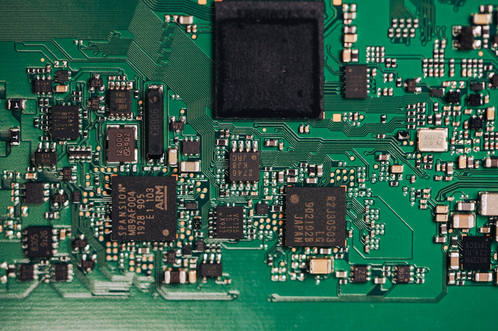
Start with drain-source voltage, including measured overshoot and suitable derating. Then examine on-resistance at the expected junction temperature, not only the 25°C headline value. Gate charge, gate-drain charge, output capacitance, reverse-recovery behavior, package inductance, thermal resistance, safe operating area, avalanche capability, and driver compatibility can all be decisive.
A device with lower RDS(on) may carry more charge and switch less efficiently. The best MOSFET minimizes total loss and stress in the actual circuit.
10. Why not use a zero-ohm gate resistor?
The driver, package, and MOSFET already contain impedance, so a zero-ohm external resistor does not create infinite speed. It can, however, produce unnecessarily fast edges, drain ringing, false turn-on, and higher EMI. Increasing resistance reduces gate current and slew rate, but raises switching loss and may disturb dead time.
Values such as 2.2 Ω, 10 Ω, or 47 Ω are only bench starting points. Select turn-on and turn-off resistance from waveforms, temperature, efficiency, and emissions. Split resistors and a diode are often used when the two transitions need different speeds. A gate-to-source pull-down prevents a floating gate during startup; its value must also fit driver bias and shutdown requirements.
11. Why does a flyback transformer need an air gap?
A flyback magnetic component stores energy in its magnetizing inductance. An intentional gap increases the magnetic circuit reluctance, allows the required energy storage, and controls inductance without saturating the core at the target peak current. Much of the energy is stored in the gap.
The gap also produces fringing fields. Poor winding placement near the gap can raise copper loss and local temperature, while excessive leakage inductance increases clamp loss and MOSFET stress. Gap, core shape, winding arrangement, insulation, and manufacturability have to be designed together.
12. Which inductor rating is easiest to miss?
Saturation current is frequently misunderstood. Confirm how the vendor defines it: a 10%, 20%, or 30% inductance drop leads to different published numbers. Peak current must remain within the allowable inductance roll-off at the highest operating temperature and transient condition. Also check RMS current against winding temperature rise, DC resistance at temperature, core loss at the actual ripple frequency, shielding, and bias-dependent inductance.
13. Why combine electrolytic capacitors with MLCCs?
Bulk capacitors provide energy storage and handle lower-frequency ripple. MLCCs offer low impedance at higher frequency and help close fast current loops. Their roles overlap but are not identical. MLCC capacitance can fall sharply with DC bias, while very low ESR can reduce damping and expose resonances. Electrolytic ESR may be useful to the control loop in older regulator designs, yet its lifetime and ripple-current limit require attention.
14. Is capacitance and voltage rating enough for an electrolytic capacitor?
No. Calculate RMS ripple current, estimate hot-spot temperature, and use the manufacturer’s life model. Check ESR versus frequency and temperature, surge voltage, physical vent clearance, mounting orientation, and expected ambient life. Parallel capacitors can share ripple current, but sharing depends on ESR, layout resistance, and temperature; it should not be assumed to be equal.
15. What does an RCD clamp do, and can I oversize it?
An RCD clamp absorbs energy associated mainly with transformer leakage inductance and limits the primary switch voltage after turn-off. More capacitance or a lower clamp voltage may reduce the peak, but it increases dissipation or changes resistor stress. Too little damping leaves dangerous ringing; too much wastes power and can overheat the clamp. Measure the leakage-related waveform, calculate energy over the switching rate, check worst-case line and load, and verify temperature.
PCB layout and isolation
16. What is the first PCB layout rule?
Minimize the area and inductance of loops carrying high di/dt current. In a buck converter, the input capacitor, high-side switch, low-side switch or diode, and return path form the critical input loop. In a flyback, the primary switch loop and secondary rectifier loop both matter. Place the relevant bypass capacitors at the switching devices, use short wide connections, and avoid unnecessary vias in these loops.
17. How should the switch node be routed?
Keep its copper area only as large as electrical current and thermal requirements justify. A large high-dv/dt surface capacitively couples noise into feedback, control, chassis, and adjacent layers. Keep it away from feedback dividers, current-sense traces, optocoupler compensation, connectors, and enclosure metal. “Never pour copper” is too absolute: some devices need copper for heat spreading. The engineering task is to satisfy thermal limits without turning the node into an antenna.
18. How should power ground and signal ground be connected?
Follow the controller data sheet and evaluation-board current paths. The objective is to stop pulsating power current from sharing impedance with sensing and control returns. Kelvin-connect current-sense and feedback returns where required. A single-point connection can work in many low-frequency arrangements, while a well-designed continuous ground plane may be better for high-frequency return current. Blindly splitting a plane can force noise around a slot and make EMI worse.
19. What matters in the primary-to-secondary isolation region?
Creepage and clearance must meet the actual insulation standard, working voltage, overvoltage category, pollution degree, material group, altitude, and insulation type. Slots can increase creepage when designed correctly, but copper, component bodies, mounting hardware, conductive contamination, and assembly tolerances still count. Do not use silkscreen as insulation. Also review transformer construction, optocoupler or digital-isolator ratings, Y-capacitor safety class, and hipot test requirements.
Ripple, audible noise, and abnormal output
20. Why does measured ripple look tens or hundreds of millivolts too high?
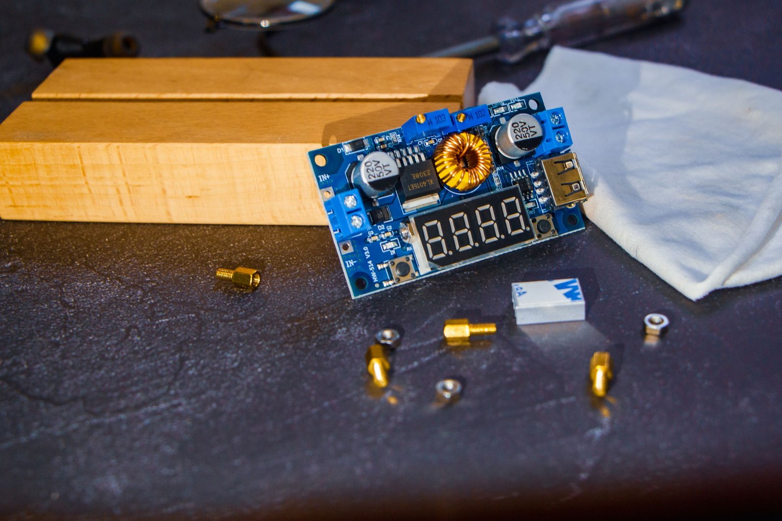
A long probe ground lead forms an inductive pickup loop and can display switching transients that are largely measurement artifacts. Probe directly across the output capacitor with a ground spring or tip-and-barrel connection. For very low levels, a short 50 Ω coaxial connection with DC blocking and proper termination is stronger than a general-purpose 10× probe.
AC coupling and a 20 MHz bandwidth limit are common specification conditions, but use the bandwidth required by the product specification and record it. A 1× probe improves sensitivity but often has lower bandwidth and greater capacitance. State input voltage, load, probe method, measurement point, temperature, and bandwidth with every ripple result.
21. What causes audible whining?
First identify the operating condition: startup, no load, a particular load band, or line-voltage range. Burst-mode repetition or a limit-cycle oscillation can enter the audible band. Transformer windings and cores can move through electromagnetic forces and magnetostriction; ceramic capacitors can move through the piezoelectric effect. Poor loop stability may modulate the converter at an audible frequency.
Use electrical measurements to find the excitation before applying varnish or adding a preload. Mechanical treatment will not cure an unstable loop, and a dummy load may waste unacceptable standby power.
22. Why can no-load output voltage rise?
Possible causes include insufficient minimum load, burst-mode energy packets, transformer parasitic coupling, rectifier leakage, auxiliary-winding regulation error, or a feedback path that loses authority. Verify the controller’s intended no-load mode and standby target. Then inspect the reference, optocoupler, TL431 bias current, divider, leakage, and dummy-load provision. Do not add a bleeder until its continuous loss is acceptable.
23. Why does output voltage drop under load?
Measure where the voltage is lost. Cable and connector resistance can imitate poor regulation. Inside the supply, likely causes include current limit, inductor saturation, excessive winding resistance, rectifier drop, inadequate input bulk voltage, thermal foldback, insufficient duty-cycle range, or a compensation problem during a transient. Compare DC droop with transient recovery; they point to different mechanisms.
| Symptom | First measurement | Likely direction |
|---|---|---|
| Slow DC droop as load rises | Input bus, duty cycle, current-limit signal | Copper loss, current limit, duty limit, rectifier drop |
| Sudden collapse and restart | VCC and protection pins | UVLO, overload, hiccup, auxiliary-winding problem |
| Brief undershoot then recovery | Output and load current together | Output capacitance, ESR, loop bandwidth |
| Excess heat before droop | Component temperatures and current waveform | Saturation, RMS loss, poor cooling |
Feedback and loop stability
24. Which loop-stability targets matter?
Phase margin around 45° is a common minimum target, and many robust designs aim higher. Gain margin around 10 dB to 12 dB is often used as a review criterion. Neither number alone guarantees good transient behavior. Check crossover relative to switching frequency, plant poles and zeros, sampling effects, optocoupler variation, output-capacitor tolerance, and operating mode.
The often-quoted crossover target of one-fifth to one-tenth of switching frequency is only an upper starting region for many regulators. A CCM boost or flyback may require a much lower bandwidth because crossover should remain well below its right-half-plane zero. Measure across low/high line, minimum/nominal/full load, temperature, and component corners.
25. Where should I start when a TL431 and optocoupler loop chatters or whines?
Confirm bias before tuning compensation. A TL431 needs sufficient cathode current and the optocoupler must remain in a predictable current-transfer range. Measure VCC, reference voltage, optocoupler current, gate waveform, and output behavior. Then review the compensation network against the power-stage model.
Making the compensation capacitor “larger for stability” can lower bandwidth and create poor transient response; making it smaller can raise crossover into an unsafe region. Optocoupler CTR spread and aging belong in the design margin.
26. What is a right-half-plane zero, and where does it appear?
A right-half-plane (RHP) zero initially moves the output in the opposite direction to the control action, adding gain while reducing phase. CCM boost, buck-boost, SEPIC, and flyback power stages can exhibit it. The loop crossover must remain comfortably below the lowest expected RHP-zero frequency. A DCM flyback generally does not have the same RHP zero, although sampling, output pole movement, optocoupler delay, and mode transitions still limit bandwidth.
Failure analysis, protection, and EMC
27. What commonly destroys a MOSFET at power-up?
Separate electrical overstress from thermal overstress. Common mechanisms include leakage-inductance overshoot, transformer saturation, excessive duty cycle, cross-conduction, gate ringing, false turn-on, inadequate driver UVLO, avalanche accumulation, current-sense delay, startup into overload, and a shorted secondary device. A poor loop layout increases several of these stresses.
Use a current-limited source or series protection for initial debugging. Capture gate-source voltage, drain-source voltage, current, controller VCC, and protection timing with appropriately rated isolated or differential probes. Replace the failed MOSFET only after checking its gate resistor, driver, current-sense path, clamp, rectifier, and transformer.
28. Why does a supply repeatedly restart because VCC never establishes?
The startup source charges VCC to the controller’s turn-on threshold, after which an auxiliary winding or bias supply must take over before VCC falls to UVLO. Restart cycling occurs when this handoff fails. Check startup resistance and dissipation, VCC capacitance, controller consumption, auxiliary winding polarity, rectifier orientation, turns ratio, loading, and UVLO thresholds. Protection events can produce the same symptom, so correlate VCC with current-sense and fault pins.
29. What should happen during an output short circuit?
For many isolated industrial supplies, hiccup protection is a sound default because it limits average device temperature while periodically testing whether the fault has cleared. Other valid strategies include constant-current limiting, foldback, latch-off, or timed shutdown. The required behavior depends on the load, cable energy, restart safety, redundancy architecture, and product standard. Verify the worst case at high line, hot ambient, and with a partial short, which can be more stressful than a dead short.
30. How should conducted or radiated EMI be debugged?
Start with measurement discipline and noise classification. A LISN and compliant receiver or spectrum analyzer are used for conducted emissions; current probes and near-field probes help locate paths. Determine whether the dominant mechanism is differential mode, common mode, or radiation from a cable or enclosure seam.
Then work from source to path to victim. Reduce hot-loop and switch-node area, damp real ringing, control edge rate where loss allows, and improve return paths. The input filter must be placed so noise cannot bypass it through traces or capacitance. Across-line X capacitors and common-mode chokes are normally on the mains side in an approved, safety-compliant network; exact order around fuse, surge protection, choke, bridge, and bulk capacitor depends on the architecture. Safety-rated Y capacitors and transformer shielding can reduce common-mode noise, but leakage current and touch-current limits constrain them.
31. How can input inrush current be limited?
An NTC thermistor is simple and inexpensive, but it runs hot, wastes power, and may not reset after a brief power interruption. Higher-power systems often bypass the NTC with a relay after charging the bulk capacitor. Active MOSFET or thyristor circuits provide more controlled behavior but add fault modes and control requirements. Select the method from bulk capacitance, line range, repetitive-cycle requirement, fuse I²t, bridge rating, ambient temperature, and brownout behavior.
Design and production practice
32. What are the benefits and penalties of higher switching frequency?
Higher frequency can reduce the required magnetic energy storage and filter size, and it can move fundamental noise away from an application band. It also raises switching, gate-drive, and often core loss; makes parasitics more influential; and can increase EMI. There is no universal “industrial” or “consumer” frequency range. Modern converters span from tens of kilohertz to several megahertz. Choose frequency with the semiconductor technology, magnetic material, efficiency target, acoustic behavior, size, and compliance plan in view.
33. How does a prototype BOM differ from a production BOM?
Price breaks are only one difference. Production exposes tolerance stacks, approved-vendor substitutions, component lifecycle, test time, transformer repeatability, soldering limits, traceability, and counterfeit risk. A part that works in ten prototypes may fail when optocoupler CTR, magnetic gap, capacitor ESR, MOSFET threshold, and ambient temperature all reach an unfavorable corner.
Create electrical and mechanical acceptance criteria for custom magnetics. Define which substitutions require requalification. Confirm creepage, thermal margin, protection, and EMC on production-representative units, not a hand-tuned golden sample.
34. What is a complete switching power supply design flow?
Begin with a written specification that includes abnormal conditions and compliance requirements. Select the topology and control method, calculate stress and loss, design magnetics, choose parts with corner margin, and build the schematic around current paths and protection. Lay out the power stage before routing convenience signals.
Bring up the board with limited energy. Verify startup, steady-state waveforms, loop stability, ripple, load transients, protection, temperature, and EMI across the operating envelope. Review tolerance and supplier variation before releasing the production BOM, test fixture, and work instructions.
| Review stage | Evidence to retain | Release question |
|---|---|---|
| Specification | Input/output range, transients, isolation, environment, standards | Are normal and abnormal conditions explicit? |
| Calculation | Stress, loss, magnetics, thermal and tolerance analysis | Are worst-case corners covered? |
| Layout | Annotated hot loops, isolation distances, thermal paths | Do return currents follow the intended path? |
| Verification | Waveforms, Bode plots, ripple setup, thermal images, protection tests | Is every result tied to a condition and limit? |
| Production | Approved BOM, transformer criteria, test limits, change control | Can another factory build the same behavior? |
Five checks worth keeping beside the oscilloscope
Report ripple as peak-to-peak voltage with bandwidth, load, and probe method.
Use a rectifier technology whose speed, voltage, current, temperature, and recovery behavior suit the switching node; a slow mains rectifier is not a high-frequency freewheel diode.
Treat Y-capacitor value as a safety and leakage-current decision, not a free EMI adjustment.
Use a ground spring, tip-and-barrel method, or terminated coax for millivolt-level ripple; a 10× probe can bury the signal in the noise floor.
Test no load for standby behavior and rated load for useful ripple data. Also test the load points where mode transitions occur.
Conclusion
Good switch-mode power design is less about memorizing “correct” component values and more about keeping the energy path, control loop, measurement setup, and fault behavior visible at every stage. A design that looks clean at nominal input and room temperature is unfinished until its worst corners have been measured.
For OEMs that need an industrial AC/DC or DC/DC supply rather than a custom converter, SIPURUI can help narrow the electrical, environmental, installation, and compliance requirements before model selection. Bring the real load profile and enclosure constraints; they are more useful than wattage alone.