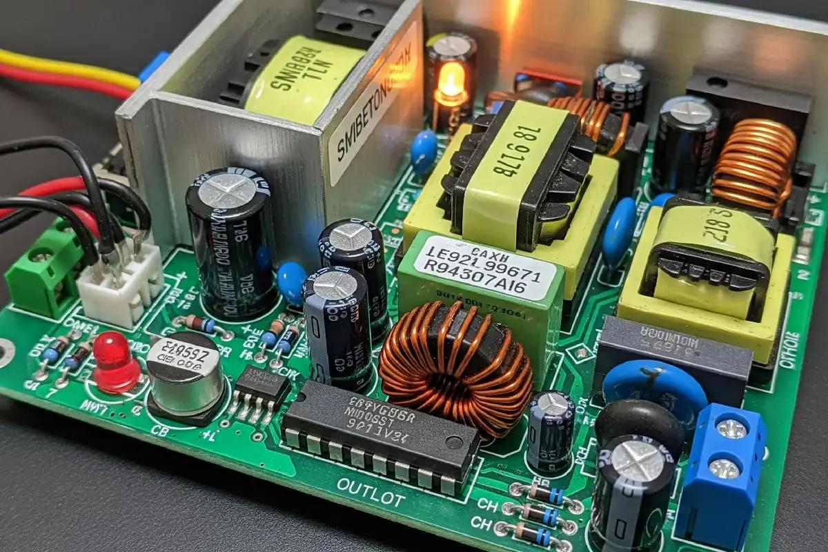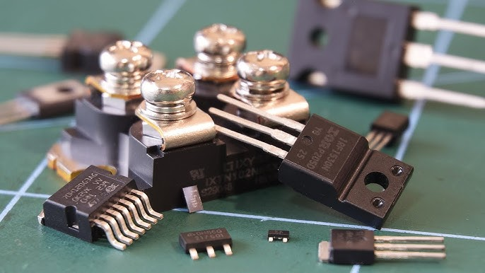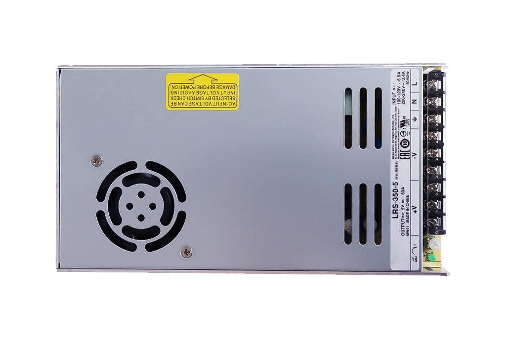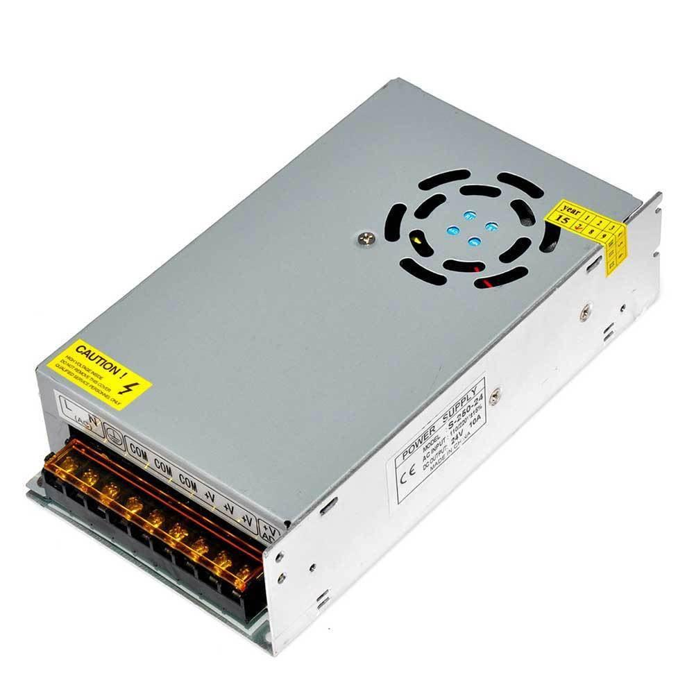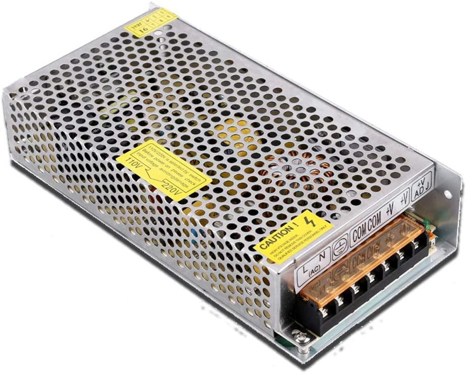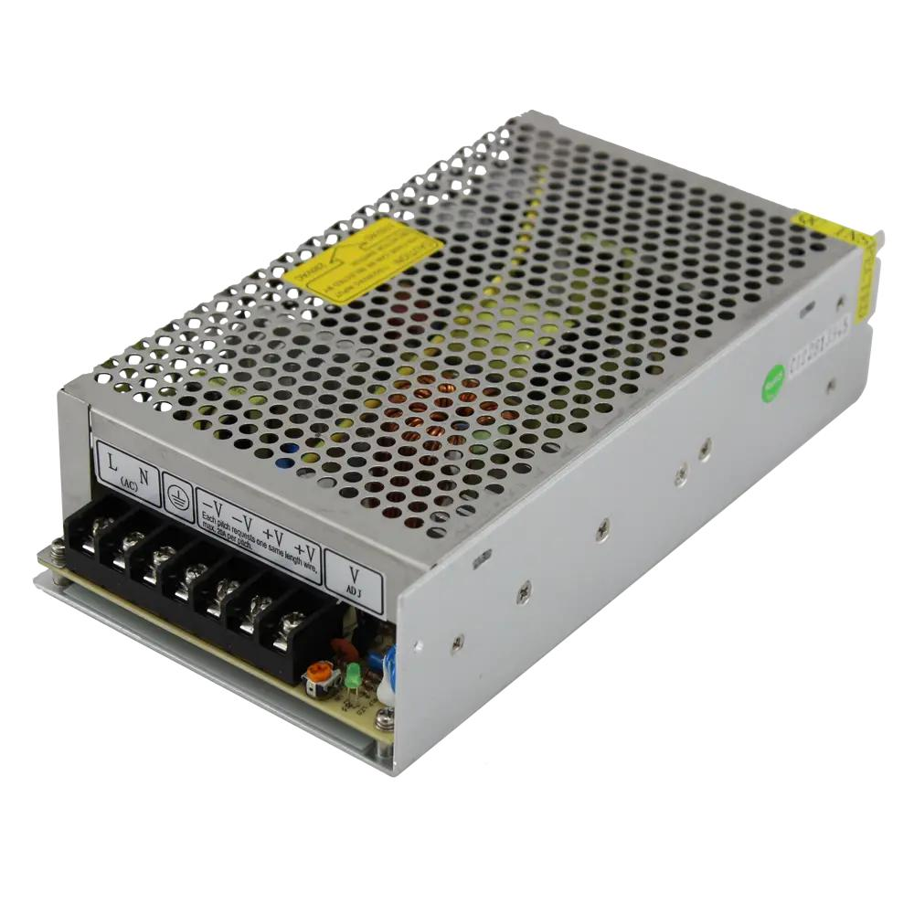


Anyone who has worked on switching power supply development has probably experienced this situation before: the schematic looks correct, simulation results appear stable, component parameters are carefully selected, yet the finished prototype still produces unexpected noise, excessive temperature rise, or unstable output during testing. Sometimes the converter works under light load but behaves differently under full load. Sometimes efficiency falls below expectations. Sometimes EMI becomes difficult to control. In many of these cases, the real issue is not hidden inside the circuit diagram. It is hidden in the PCB layout.
In switch mode power supply design, PCB layout is not simply the final step of placing components and routing copper traces. It is an essential part of the power design itself. Once energy begins moving through the board at high switching frequency, layout becomes responsible for controlling current paths, heat flow, electromagnetic radiation, and signal stability. A well-designed layout helps every component perform as intended. A poor layout can turn a solid design into a difficult product.
At SIPURUI, we often see that layout decisions made in the early design stage have direct impact on the final reliability of the power supply. Whether the application is an enclosed AC-DC switching power supply, a compact industrial control module, or an open-frame converter for embedded equipment, the PCB is never just a platform that holds components. It becomes part of the electrical system.
Why High-Frequency Switching Makes Layout More Critical
A switching power supply operates differently from ordinary analog circuitry because energy is transferred through continuous switching. The MOSFET repeatedly turns on and off, often hundreds of thousands of times every second. This fast switching action is what gives the power supply high efficiency, but it also introduces rapid voltage transitions, high current pulses, magnetic coupling, and electromagnetic noise.
These effects do not stay inside the schematic. They interact with the copper traces, the spacing between components, the size of the ground plane, and the physical structure of the PCB.
That is why two switching power supplies using the same controller and identical component values can still behave completely differently once assembled. One may run cool and stable with excellent EMC performance. The other may generate switching spikes, audible noise, or excessive ripple. The difference often comes from layout.
Current Always Follows a Path—and That Path Matters
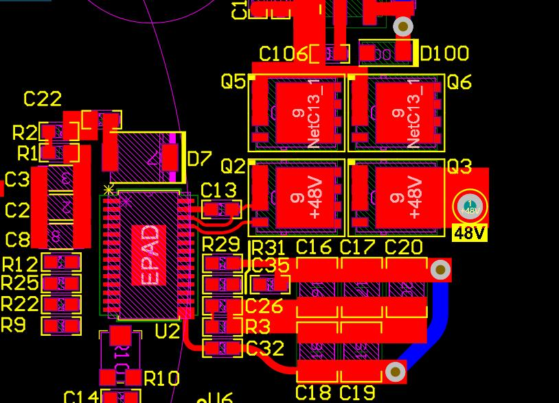
One of the most important realities in switching power supply PCB design is that current does not simply move from one component to another. It always travels in a loop. Every switching cycle creates a current path through the input capacitor, switching transistor, magnetic component, output rectifier, and return ground.
If that loop is physically large, it creates problems.
The larger the current loop becomes, the greater the parasitic inductance. As parasitic inductance increases, switching edges become noisier. Voltage overshoot becomes more noticeable. Ringing appears more easily. Electromagnetic radiation increases. What looks electrically correct in the schematic begins behaving very differently on the real board.
This is why compact placement of power components matters so much.
The input capacitor should sit as close as possible to the switching stage. The transformer or inductor should be positioned so energy transfer paths remain short and direct. Output capacitors should stay close to the rectifier stage to reduce ripple current loop length. Short copper paths lower impedance, reduce switching noise, and improve efficiency.
A clean switching loop is often the foundation of a stable power supply.
Ground Design Is More Than a Reference Plane
Ground is often treated as something simple, but in switching power supply layout it requires careful planning.
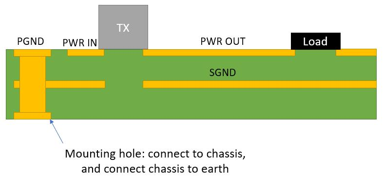
Although the schematic may show a common ground symbol across the design, the real PCB behaves differently. High-current return paths carry switching energy. Feedback circuits carry low-level analog signals. PWM control circuits rely on a clean reference voltage. If these share noisy return paths without control, switching noise can interfere with sensing and regulation.
When this happens, the power supply may appear electrically functional while still suffering from unstable performance under dynamic load conditions.
Good grounding helps prevent this.
In many SIPURUI power supply layouts, the noisy power ground and sensitive control ground are carefully organized so switching return current does not pass through signal reference areas. This allows the controller to sense output conditions accurately while keeping the switching stage stable under load changes.
Proper grounding is often invisible in the finished product, but it strongly influences long-term reliability.
The Noisiest Area on the Board Usually Comes from the Switching Node
Every switching power supply has a location where voltage changes extremely fast. In many designs this is the switching node connected to the MOSFET drain or SW pin of the converter stage. This area can become the strongest source of EMI on the PCB.
Because voltage at this node rises and falls rapidly, it creates strong electric field radiation around nearby copper.
If sensitive feedback traces pass too close to it, noise coupling becomes possible. If control traces are routed under the magnetic component, the switching field may interfere with the feedback loop. If copper around the switching node is unnecessarily large, radiated EMI often becomes worse.
For that reason, experienced layout designers usually keep switching node copper compact and controlled. Sensitive traces are routed away from it. Signal lines are isolated wherever possible. Layout is arranged to keep the noisy power stage contained.
Small improvements here often produce major improvements during EMC testing.
Thermal Performance Begins with Layout
Heat is unavoidable in switching power conversion.
Even efficient power supplies produce losses through MOSFET switching, transformer copper loss, core loss, rectifier loss, and conduction resistance across the power stage. Once heat is created, it must be removed effectively.
If not, internal temperature rises and component lifetime decreases.
Electrolytic capacitors age faster at elevated temperature. Semiconductors experience more thermal stress. Magnetic materials become less efficient. Long-term reliability begins to decline.
This is why PCB layout must also be treated as a thermal design tool.
Copper pours are not only used for conductivity. They are also used to spread heat. Thermal vias beneath power devices help transfer heat between PCB layers. Component spacing improves airflow. Copper thickness affects both current handling and heat dissipation.
In many SIPURUI switching power supply designs, the PCB itself becomes part of the thermal structure. Good thermal layout reduces hot spots and improves service life without increasing product size.
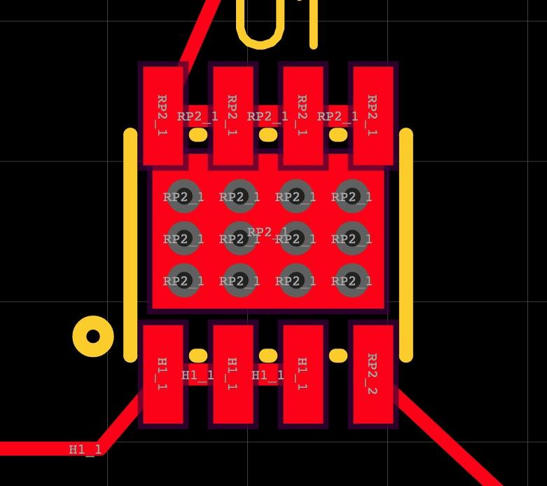
Good Placement Leads to Better Power Supply Performance
Component placement influences almost everything inside a switching power supply. It affects current flow, thermal distribution, noise coupling, manufacturability, service access, and electrical performance.
The transformer cannot simply be placed wherever space is available. Its position affects isolation spacing, magnetic behavior, and routing efficiency.
Input capacitors influence ripple suppression depending on distance from the switching stage.
Output capacitors directly affect output ripple and transient response depending on their location relative to the rectifier.
Feedback networks perform best when kept quiet and separated from noisy switching areas.
Well-designed placement makes routing easier because the energy path already makes sense before routing begins.
This is often the difference between a layout that looks organized and one that actually performs well.

Final Thoughts
A switching power supply can only perform as well as the PCB beneath it allows.
The schematic defines the circuit, but layout defines how that circuit behaves in real operating conditions. Once current begins switching at high frequency, every millimeter of copper starts affecting performance. Noise, thermal behavior, EMI, efficiency, and reliability all become connected to layout decisions.
That is why PCB layout remains one of the most important parts of switching power supply engineering.
At SIPURUI, we believe that reliable power supply design begins long before testing and continues far beyond schematic capture. It extends into copper geometry, grounding strategy, component placement, thermal planning, and careful control of switching energy throughout the board.
Because in the end, the PCB is not just supporting the power supply.
It is part of the power supply itself.