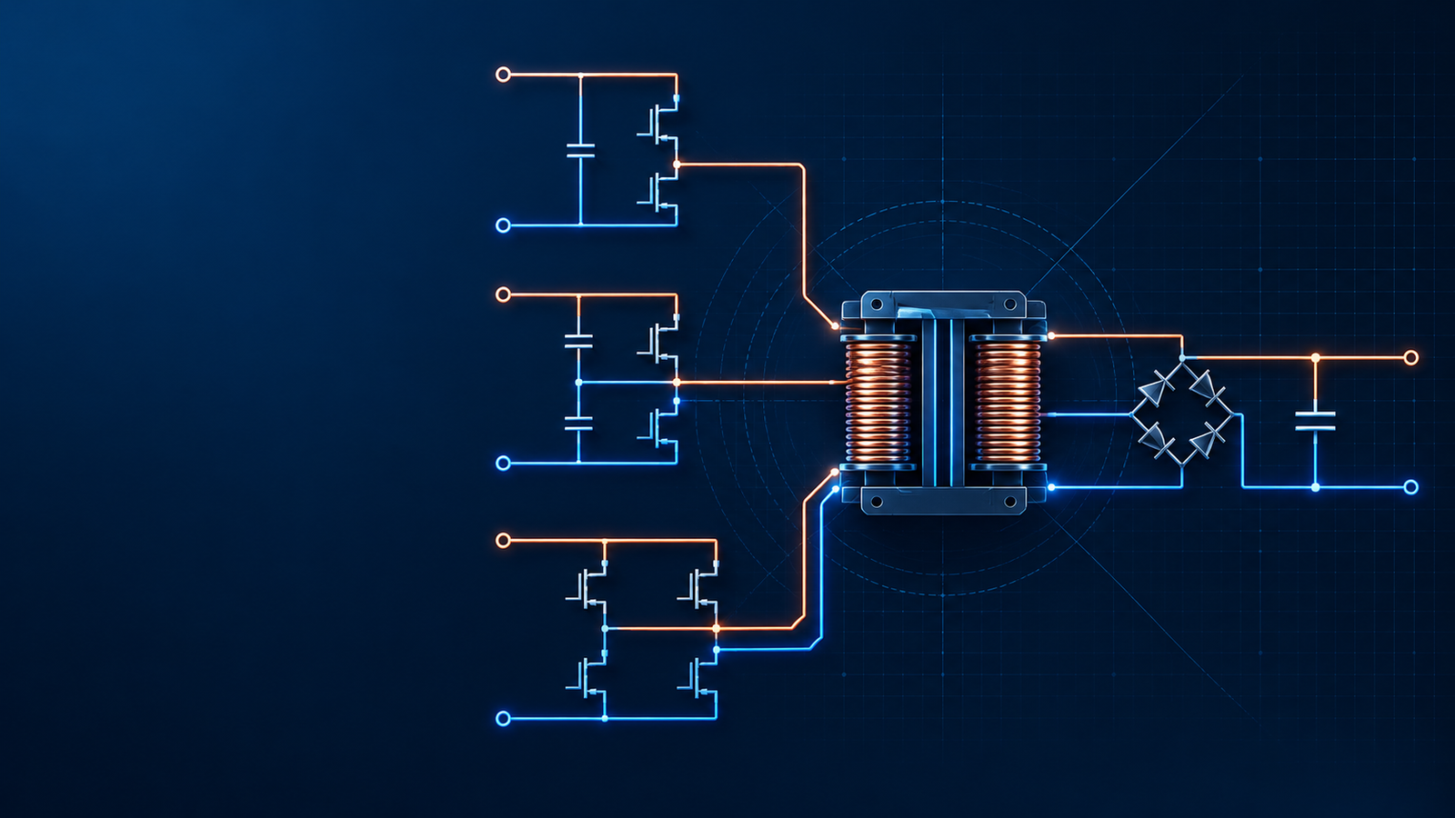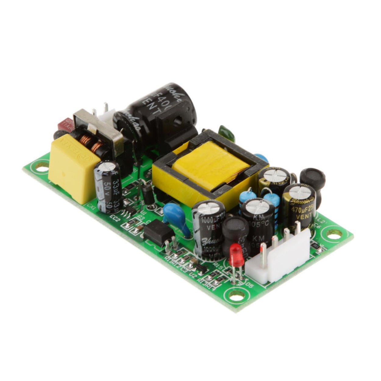
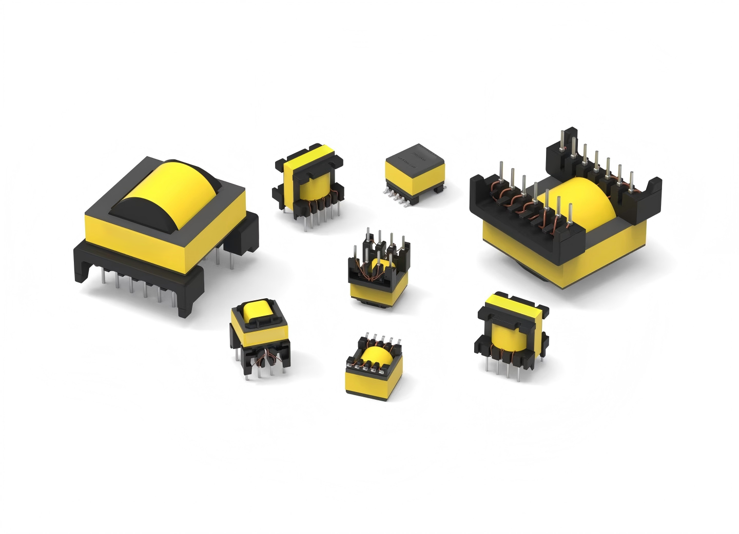
A flyback transformer is better understood as a coupled inductor. During MOSFET on-time, the primary stores energy in the magnetic field; during off-time, that energy moves to the secondary. That distinction matters. A design can have the right turns ratio and still fail because its magnetizing inductance, air gap, insulation system, or winding arrangement is wrong.
Overview
A flyback transformer is better understood as a coupled inductor. During MOSFET on-time, the primary stores energy in the magnetic field; during off-time, that energy moves to the secondary. That distinction matters. A design can have the right turns ratio and still fail because its magnetizing inductance, air gap, insulation system, or winding arrangement is wrong.
This guide works through a universal-input, 12 V/2 A example from first-pass assumptions to a hand-wound prototype. It also corrects a common specification error: 12 V × 2 A is 24 W, not 30 W. If 30 W is the actual requirement, the output current, current limit, wire sizes, core loss, and thermal verification must all be recalculated.
The numbers below are a defensible starting point, not a production transformer specification. Controller current limits, brownout behavior, rectified-bus ripple, ferrite grade, bobbin dimensions, insulation requirements, and measured temperature rise can move the final design.
1. Freeze the electrical boundary conditions
The worst case for primary current and saturation usually occurs near the lowest rectified bus voltage, while MOSFET drain stress is checked at the highest bus voltage. Treating one line condition as “worst” for every calculation is a shortcut that creates blind spots.
| Design item | First-pass value | Why it matters |
|---|---|---|
| AC input | 85–265 VAC | Universal mains range |
| Minimum bulk-bus voltage | 90 VDC | Low-line valley assumption; verify with the real input capacitor and hold-up requirement |
| Maximum bulk-bus voltage | 375 VDC | High-line stress calculation |
| Output | 12 V, 2 A | 24 W rated output |
| Estimated efficiency | 85% | Gives about 28.2 W input at full load |
| Switching frequency | 65 kHz | Nominal full-load design frequency |
| Target maximum duty cycle | about 0.44 | Leaves controller and transient margin |
| Secondary diode drop | 0.5 V | Initial Schottky estimate at operating current |
| Trial core | PQ20/16 ferrite set | Compact candidate; final acceptance depends on loss and thermal testing |
| Effective core area, Ae | 62 mm² | Use the selected manufacturer’s current datasheet |
| Trial flux excursion | 0.18 T | Conservative first pass for ferrite at elevated temperature |
The 90 V minimum bus is not simply 85 VAC multiplied by √2. Rectifier drop and twice-line-frequency capacitor ripple pull the valley lower than the peak. Measure or simulate the front end instead of copying 90 V into every universal-input design.
2. Set the reflected voltage before choosing the turns
The reflected output voltage sets several linked quantities: duty cycle at low line, MOSFET voltage at high line, transformer turns ratio, secondary diode reverse voltage, and primary current. A useful initial value for this example is approximately 75 V.
At the boundary between energy storage and energy transfer, the ideal duty ratio is:
D = VOR / (Vin + VOR)
With 90 V at the bulk-capacitor valley and 75 V reflected to the primary:
D = 75 / (90 + 75) = 0.455
The integer turns selected later produce a reflected voltage close to 71 V, so the actual first-pass duty ratio becomes about 0.442. This is internally consistent with the intended 0.44–0.45 range.
A 90 V reflected voltage and a 0.45 duty ratio do not fit a 90 V minimum bus in the ideal volt-second relationship. Those three values are sometimes copied into design notes together, but they cannot all describe the same operating point.
For a 650 V MOSFET, an approximate high-line check is:
VDS ≈ Vbulk,max + VOR + Vspike
Using 375 V and about 71 V leaves roughly 204 V for leakage spike, ringing, tolerances, and design margin. That is not permission to accept a 200 V spike. It shows why the clamp must be designed and then measured with the correct high-voltage probing technique.

3. Choose a core from manufacturer data, not a generic power table
Area-product charts are useful for screening core sizes, but the constant changes with topology, waveform, units, current density, fill factor, temperature rise, and cooling. A bare statement such as “the required AP is 0.42 cm⁴” cannot be audited unless its equation and units are fully defined.
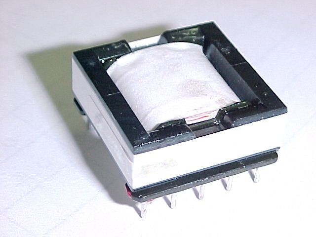
PQ20/16 is a plausible trial size for this 24 W design. TDK lists PQ20/16 parts in several power ferrite materials, with ungapped AL values that vary by material. The actual bobbin winding width and usable window must come from the matching bobbin drawing. Before approving the core, check:
loss density at the calculated flux waveform and worst core temperature;
space for primary, insulation, secondary, auxiliary winding, margins, and lead dress;
creepage and clearance for the applicable safety standard;
availability of a controlled gapped core or a repeatable grinding process;
temperature rise in the final enclosure, not only on an open bench.
If the PQ20/16 window fails the insulation or copper-fill check, move up a size. Forcing the windings into a marginal bobbin usually raises leakage, capacitance, copper loss, or safety risk.
4. Calculate magnetizing inductance and peak current together
For a boundary-mode first pass, the input energy per switching cycle is:
Pin = ½ × Lp × Ipk² × fs
Primary current rises during on-time according to:
Ipk = Vin × D / (Lp × fs)
Combining the two equations gives:
Lp = Vin² × D² / (2 × Pin × fs)
Using 90 V, D = 0.442, Pin = 24/0.85 = 28.2 W, and 65 kHz gives:
Lp ≈ 432 µH
The corresponding peak current is:
Ipk ≈ 90 × 0.442 / (432 µH × 65 kHz) ≈ 1.42 A
These two numbers belong together. A 600 µH primary operated at the same 90 V, duty ratio, and frequency reaches only about 1.02 A and transfers roughly 20 W of input power in boundary mode. It cannot simultaneously be a 24 W output design at 85% efficiency without a different conduction mode, duty ratio, frequency, or current waveform.
This example uses boundary-mode equations because they make the energy balance transparent. A fixed-frequency CCM design needs a chosen ripple ratio and nonzero valley current; a controller with frequency foldback or quasi-resonant valley switching needs its own operating-law calculation.
5. Determine primary, secondary, and bias turns
The primary turns come from the allowed flux change during on-time:
Np ≥ Vin,min × D / (fs × ΔB × Ae)
With Ae = 62 mm² and ΔB = 0.18 T:
Np ≥ 90 × 0.442 / (65 kHz × 0.18 T × 62 mm²) ≈ 55 turns
Choose 57 turns for a little margin and a convenient integer ratio. This estimate must be repeated with the actual Ae tolerance and worst-case frequency.
The secondary turns follow from the reflected voltage:
Np/Ns = VOR / (Vo + Vf)
Ten secondary turns with 57 primary turns give:
VOR = (57/10) × (12 + 0.5) ≈ 71.3 V
At a nominal 15 V bias supply with an estimated 0.7 V rectifier drop:
Naux ≈ Ns × (Vaux + Vf,aux) / (Vo + Vf,sec)
This yields about 12.6 turns, so 13 turns is a sensible prototype value. The bias voltage must be checked at startup, no load, full load, low line, and high line. Leakage spikes and cross-regulation often make the measured value differ from the simple turns ratio.
| Winding | Prototype value | Electrical note |
|---|---|---|
| Primary | 57 turns | Target Lp about 430 µH; split winding may reduce leakage |
| Secondary | 10 turns | 12 V output with initial 0.5 V diode allowance |
| Bias | 13 turns | Initial target near 15 V; tune after bench measurement |
| Effective reflected voltage | 71.3 V | Based on the chosen integer turns |
| Low-line duty estimate | 0.442 | Ideal first pass at 90 V bus valley |
6. Set the AL target, then obtain the gap by measurement
The target gapped inductance factor is more useful for procurement than a universal spacer thickness:
AL,target = Lp / Np² = 432 µH / 57² ≈ 133 nH/turn²
If the air gap dominates the magnetic reluctance, a rough total effective gap is:
lg ≈ µ0 × Np² × Ae / Lp
This gives about 0.59 mm. Fringing, distributed gap geometry, finite ferrite permeability, and whether the gap is placed on the center leg or shared between mating surfaces change the mechanical result. Use 0.5–0.6 mm only as a machining starting region, then gap the assembled core until the measured primary inductance reaches the target.
A fixed “0.3 mm gap for PQ20/16” is not a transferable rule. Different turns, inductance, ferrite, and grinding geometry require different gaps. Spacers on all legs also create external fringe fields and a different reluctance path than a controlled center-leg gap.
7. Size copper from RMS current and winding fit
Wire selection based only on output DC current understates the heating in a flyback winding. At the boundary point, the primary current is triangular during MOSFET on-time:
Ipri,rms = Ipk × √(D/3) ≈ 0.54 A
The secondary peak current is approximately:
Isec,pk = Ipk × Np/Ns ≈ 8.1 A
For a triangular secondary pulse over the off-time:
Isec,rms ≈ Isec,pk × √((1-D)/3) ≈ 3.5 A
At an initial current density near 4 A/mm² for the primary and 4–5 A/mm² for the secondary, practical starting choices are two parallel 0.30 mm primary wires and three parallel 0.55 mm secondary wires. The individual strand diameters also help with skin and proximity effects at 65 kHz. Final copper loss must use mean length per turn, hot copper resistance, and the actual AC waveform.
| Winding | Estimated RMS current | Practical starting conductor | Why the original single-wire shortcut fails |
|---|---|---|---|
| Primary | 0.54 A | 2 × 0.30 mm magnet wire in parallel | A single 0.21 mm wire has only about 0.035 mm² copper area and would run at excessive current density |
| Secondary | 3.5 A | 3 × 0.55 mm, or qualified equivalent foil/litz arrangement | A single 0.55 mm wire is sized for far less than the pulsed RMS current |
| Bias | Controller-dependent | 0.20–0.25 mm starting range | Verify rectifier pulse current and regulation rather than assuming 0.1 A DC |
Run a winding-build calculation using insulated outside diameters, not bare copper diameters. Include tape thickness, margins, sleeving, crossover space, and manufacturing tolerance.
8. Build an insulation system before winding copper
Offline transformer construction is a safety design. “Two layers of tape” is not a universal reinforced-insulation specification. Tape material, thickness, overlap, bobbin geometry, creepage path, lead sleeving, production hipot, pollution degree, overvoltage category, and the end-product standard all matter.
Power Integrations’ construction guidance describes two common approaches: margin-wound construction using ordinary magnet wire plus controlled margins and insulation, and a triple-insulated secondary that can use more of the bobbin width. Choose the system with the safety engineer and insulation-material certifications in hand.
A sensible prototype sequence for secondary-side regulation is:
Deburr and clean the bobbin. Fit approved lead sleeving where required.
Wind 28 primary turns evenly across the available width. Avoid crossovers inside a layer.
Apply the designed basic insulation between primary sections and the secondary region.
Wind the 10-turn secondary with triple-insulated parallel conductors, keeping all strands together and observing the specified pin-side creepage.
Apply the specified reinforced-insulation build.
Wind the remaining 29 primary turns in the same electrical direction as the first section.
Place the 13-turn bias winding where the regulation and EMI plan requires. For secondary regulation it is often placed between primary and secondary; for primary-side regulation, closer coupling to the secondary may be preferable.
Terminate, sleeve, tape, assemble the gapped core, clamp or bond it, and remeasure inductance.
Splitting the primary generally reduces leakage by sandwiching the secondary between primary halves. The tradeoff is higher primary-to-secondary capacitance, which can worsen common-mode EMI. A copper shield or flux band must never form a shorted turn, and it can reduce creepage if applied carelessly.
9. Measure before applying full mains voltage
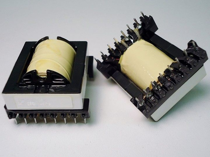
Start with low-energy tests. Confirm winding continuity, polarity, turns ratio, primary inductance, and leakage inductance before the transformer goes into the power stage. Record the test frequency and fixture because leakage readings depend on how the secondary is shorted and how the leads are arranged.
| Check | Initial target | What to do if it misses |
|---|---|---|
| Primary inductance | about 430 µH | Adjust the controlled gap; do not change turns casually because flux and ratio also change |
| Turns ratio | 57:10:13 | Verify polarity dots and counted turns with a low-voltage AC test |
| Leakage inductance | Set from clamp-loss and drain-spike budget | Improve layer coverage, shorten leads, reconsider interleaving, then retest EMI |
| MOSFET drain peak | Below the derated device limit at high line | Tune clamp/snubber and winding coupling; use a rated differential probe |
| Bias voltage | Inside controller UVLO/OVP limits across all operating points | Adjust bias turns, rectifier, filtering, or clamp coupling |
| Temperature rise | Within component and insulation-class limits | Revisit core loss, copper loss, fill, airflow, and enclosure hot spots |
| Safety tests | Per the applicable product standard | Correct insulation design; a passing low-voltage functional test is not a substitute |
For first power-up, use an isolation transformer where appropriate, a current-limited source or series protection method, a safe discharge procedure for the bulk capacitor, and probes rated for the measured common-mode voltage. A standard oscilloscope ground clip connected to the primary side can short the mains circuit through protective earth.
10. Fault patterns that point back to the transformer
Repeated startup or hiccup at low line can come from inadequate energy per cycle, a controller current limit below the calculated peak, low primary inductance, a collapsing bias winding, or excessive output load. Do not assume every startup problem means “add turns.”
A drain spike that threatens the MOSFET usually points to leakage energy, clamp design, or layout. Higher primary inductance does not automatically cure it. Audible noise can originate from loose core halves, gap-surface movement, burst-mode operation, or a control loop that modulates energy in the audible band.
High full-load temperature needs a loss split. Measure winding resistance cold and hot, estimate copper loss from RMS current, calculate core loss from the actual flux waveform and material curves, and inspect nearby heat sources. Without that split, changing wire or ferrite is guesswork.
Prototype parameter sheet
| Item | First prototype value |
|---|---|
| Rated output | 12 V, 2 A, 24 W |
| Input range | 85–265 VAC |
| Assumed bus valley / maximum | 90 VDC / 375 VDC |
| Nominal switching frequency | 65 kHz |
| Trial core | PQ20/16, verified power ferrite material |
| Primary | 57 turns, split 28 + 29 |
| Secondary | 10 turns, triple-insulated construction preferred |
| Bias | 13 turns, tune to controller requirements |
| Magnetizing inductance | approximately 430 µH at the specified test condition |
| Target gapped AL | approximately 133 nH/turn² |
| Estimated low-line peak current | approximately 1.42 A |
| Estimated flux excursion | approximately 0.18 T |
| Mechanical gap | establish by measured AL; rough calculation about 0.59 mm effective total gap |
Conclusion
A credible flyback transformer design keeps volts, seconds, joules, flux, copper loss, and insulation in the same calculation chain. In this example, that chain leads to 57 primary turns, 10 secondary turns, 13 bias turns, and roughly 430 µH, followed by a controlled gapping and validation process. It also exposes why 600 µH, 1.2 A peak, 90 V reflected voltage, and 45% duty cannot be combined casually.
For a production project, SIPURUI can review the full power-supply specification alongside transformer vendors, including operating mode, controller limits, safety construction, clamp stress, EMI behavior, and thermal margin. The prototype values here are the start of that conversation, not the end of qualification.