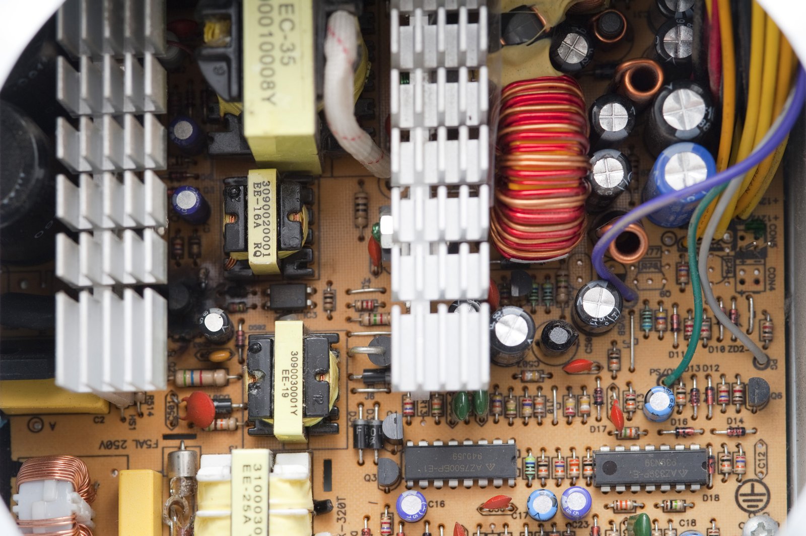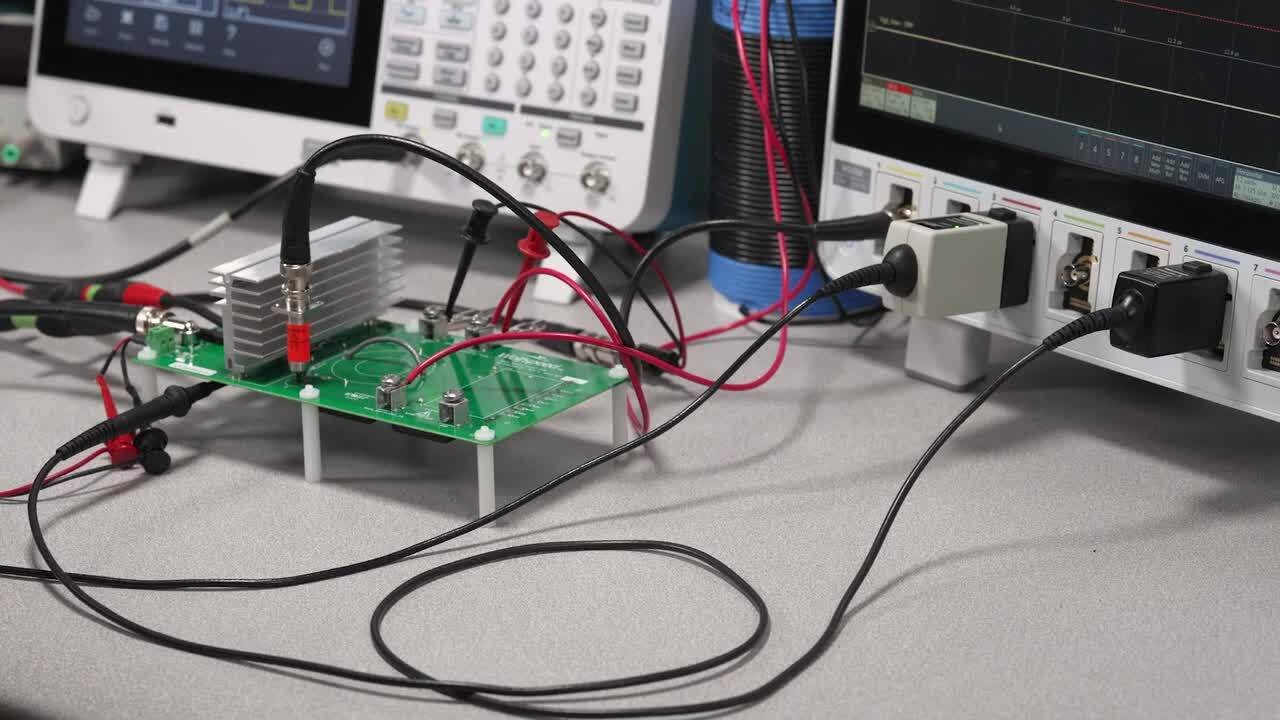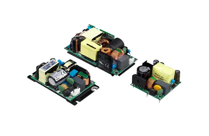
Understand how fast switching edges, parasitic coupling, transformer capacitance, PCB loops, cables, and enclosure details create conducted and radiated EMI—and how to diagnose the dominant path before choosing a fix.
Overview
A switching power supply can regulate perfectly on the bench and still fail an emissions test. The reason is that regulation and electromagnetic compatibility examine different behavior. The control loop is concerned mainly with average voltage and current. EMI testing exposes the fast edges, parasitic current paths, resonances, cable coupling, and mechanical details that the simplified schematic does not show.
For power supply engineers and equipment manufacturers, the practical lesson is straightforward: EMI is usually cheaper to prevent in the schematic, transformer, PCB, and enclosure than to repair after a certification failure. The right remedy depends on the noise mode and propagation path. Adding a larger filter at random may improve one band, do nothing in another, or even create a new resonance.
EMI, EMC, Conducted Emissions, and Radiated Emissions
Electromagnetic interference (EMI) is unwanted electrical or electromagnetic energy that can disturb another circuit or radio service. Electromagnetic compatibility (EMC) is the broader goal: equipment should operate correctly in its intended environment without emitting excessive disturbance or being unduly affected by outside disturbance.
For many mains-powered multimedia and industrial products, conducted emissions are assessed at the power port over a lower-frequency band, commonly 150 kHz to 30 MHz, while radiated emissions are evaluated from 30 MHz upward. The exact limit, detector, distance, port type, and upper frequency depend on the product family and applicable standard. CISPR 32 / EN 55032 is common for multimedia equipment; industrial, scientific, medical, automotive, household, lighting, and other equipment can fall under different standards. An EMC test plan should therefore be based on the finished product and target market, not on a generic frequency table.
| Emission category | Main propagation path | Typical diagnostic concern | Common mitigation direction |
|---|---|---|---|
| Differential-mode conducted noise | Between the two power conductors | Pulsating input current, rectifier loop, switch-current harmonics | Reduce hot-loop impedance; add a properly damped differential filter |
| Common-mode conducted noise | Both power conductors in the same direction, returning through earth or stray capacitance | Switch-node dv/dt, transformer interwinding capacitance, heatsink and chassis coupling | Control parasitic capacitance; use Y capacitors and common-mode chokes within safety limits |
| Radiated emissions | Electric or magnetic fields coupling into space and attached cables | Hot-loop area, switch-node copper, ringing, transformer fringe field, cable common-mode current | Minimize source area and ringing; control return paths; filter or shield only after locating the source |
Why Switching Power Supplies Generate Broadband Noise
The switching frequency itself is only the beginning. A 100 kHz converter does not emit solely at 100 kHz. Fast voltage and current transitions contain harmonics that extend far above the fundamental switching frequency. Edge rate, rather than nominal frequency alone, often determines how much energy reaches the tens or hundreds of megahertz range.
Fast voltage and current transitions
When a MOSFET turns on or off, current is redirected between semiconductor devices, capacitors, windings, and rectifiers in a short interval. High di/dt flowing through package, via, trace, and winding inductance produces voltage error according to V = L × di/dt. High dv/dt drives displacement current through every capacitance connected to the switching node, including capacitances that were never placed intentionally.
This is why a physically small node can cause a large problem. The drain or switching node may move by hundreds of volts in tens of nanoseconds. Even a few picofarads from that node to a heatsink, shield, secondary winding, or chassis can carry measurable high-frequency common-mode current.
Parasitic resonance and ringing
Leakage inductance, device output capacitance, diode junction capacitance, winding capacitance, and PCB inductance form resonant networks. A drain waveform that looks acceptable at a slow time scale may contain a high-frequency ringing burst at each edge. That ringing can appear as a narrow cluster of peaks in a spectrum and can efficiently excite nearby copper or cables.
Snubbers and clamps work when they address the measured resonance. An RC snubber selected by trial alone may waste power without controlling the dominant mode. A better approach is to identify the ringing frequency, determine the participating node and current loop, then tune the network with a probe setup that does not introduce its own large loop.
Transformer coupling and secondary cables
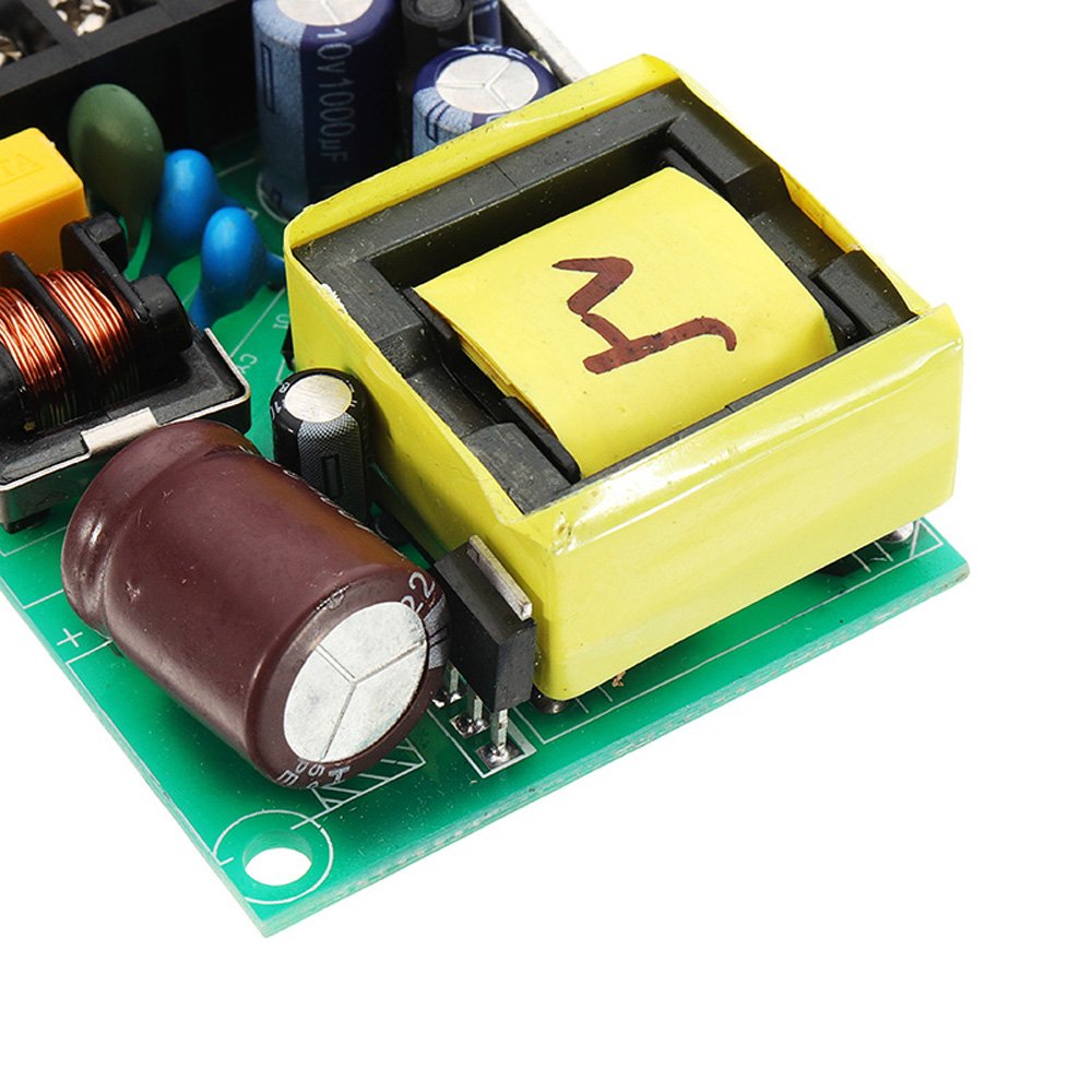
In an isolated supply, the transformer transfers more than intended power. Leakage flux couples magnetically into nearby conductors. Interwinding capacitance transfers common-mode current from the primary switch node to the secondary. Once this current reaches the output cable, the cable and load can become part of the return path and an efficient antenna.
Transformer changes involve trade-offs. Interleaving can reduce leakage inductance, but it may increase primary-to-secondary capacitance. An electrostatic shield can reduce electric-field coupling, but its connection, overlap, insulation system, and effect on capacitance must be engineered carefully. It must never create a shorted turn or compromise reinforced insulation.
Conducted EMI: Separate Differential Mode from Common Mode First
The voltage measured at a LISN or AMN port contains both modes. Treating them as one problem leads to expensive filters and slow debugging.
Differential-mode conducted noise
Differential-mode current flows out on one conductor and returns on the other. In an offline flyback supply, the rectifier and bulk capacitor draw pulsating current from the mains, while the primary switching loop draws high-frequency current from the bulk capacitor. Imperfect local decoupling and parasitic impedance allow part of this energy to reach the input port.
The first correction is physical: keep the high-frequency current local. Place the relevant film or ceramic decoupling capacitor so its loop with the switch and transformer is compact. Keep the rectifier, bulk capacitor, switching devices, and return connections arranged according to actual current paths. Then design the differential filter from the measured source and load impedances.
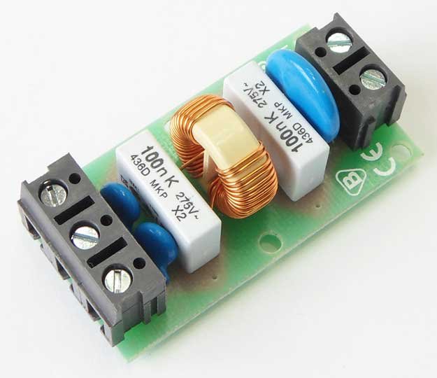
X capacitors are connected line-to-line and are safety-rated for across-the-line service. A series differential inductor or the controlled leakage inductance of a common-mode choke can add impedance. However, a C-L-C filter can interact with the converter input impedance and may need damping. Capacitor value also affects reactive input current, discharge requirements, inrush behavior, physical size, and cost. X capacitance is not the main determinant of protective-earth leakage current; Y capacitance is.
Common-mode conducted noise
Common-mode current flows in the same direction on line and neutral and returns through protective earth, chassis, load, operator-accessible capacitance, test-table ground plane, or other stray capacitances. The main driving source is usually a high-dv/dt node, not simply the converter's switching-frequency input current.
Typical coupling paths include:
primary switch node to heatsink or chassis;
primary to secondary through transformer interwinding capacitance;
primary copper to an enclosure, shield, or ground plane;
secondary circuit to the load or output cable and back through the environment.
A common-mode choke presents high impedance to same-direction noise while allowing the intended line current to pass with opposing flux. The component must be selected for current, temperature, insulation, impedance across the problem band, and the effect of its parasitic capacitance. A larger low-frequency inductance value does not guarantee better attenuation at 10 or 20 MHz.
Y capacitors provide a deliberate high-frequency return path, but they are safety-critical components. Their class, location, capacitance, creepage, clearance, leakage or touch-current contribution, and connection must comply with the product's insulation architecture and applicable safety standard. In an isolated Class II product, a primary-to-secondary Y capacitor is often used; in Class I equipment, line-to-earth arrangements may be possible. The value must come from safety and EMC calculations, not a generic maximum.
Radiated EMI: Control the Source Before Adding Metal
Radiated emissions are often caused by the same currents seen in conducted testing, but the antenna can be a PCB loop, switch-node copper, heatsink, transformer, enclosure seam, or attached cable.
Minimize the hot loop
The most effective PCB action is to identify the current that changes state abruptly and minimize the area enclosed by that loop. This is topology-specific. In a flyback primary, the critical path includes the local high-frequency input capacitor, transformer primary, MOSFET, current-sense path, and return. On the secondary, the rectifier or synchronous MOSFET and output capacitor form another pulsed-current loop.
Short traces help, but loop area and return-path continuity are more meaningful than length alone. Place the forward and return conductors close together. Avoid routing a high-dv/dt switch node over quiet control circuitry or large copper areas that increase capacitive coupling. Use the smallest switch-node copper area consistent with current and thermal requirements.
Manage edge rate and ringing deliberately
A gate resistor, split turn-on/turn-off resistance, ferrite bead, snubber, active clamp, or soft-switching topology can reduce the high-frequency energy at its source. Each has a cost. Slower switching can increase transition loss and device temperature. A snubber dissipates power. A clamp may change voltage stress and transformer behavior. Verify the trade-off at high line, low line, light load, full load, startup, and abnormal operating conditions.
Prevent cables from becoming antennas
When radiated emissions rise sharply after the output cable is attached, common-mode cable current is a strong suspect. Improve the transformer capacitance balance and secondary filtering first. A cable common-mode choke or ferrite can then be used at the connector, where it intercepts current before it spreads along the cable. Long leads between the filter and connector can bypass the intended benefit.
Use shielding with a defined return connection
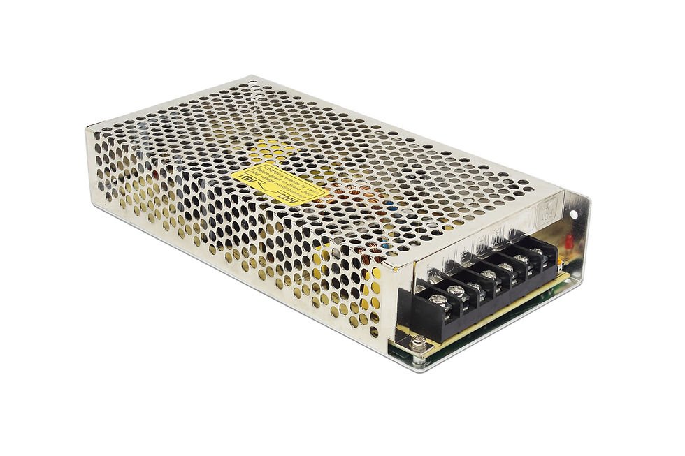
Shielding is effective only when induced current has a controlled low-impedance return. A floating metal cover can resonate or capacitively couple noise elsewhere. A shield connected by a long pigtail has substantial high-frequency inductance. Enclosure seams, cable exits, ventilation openings, and bonding methods often determine performance above 100 MHz. Shielding should follow source localization, not replace it.
A Practical Pre-Compliance Debugging Workflow
Good EMI debugging changes one variable at a time and records the result. The aim is to identify the source, coupling path, and antenna or receiving port before committing to a production change.
1. Reproduce the operating condition
Record input voltage, load, operating mode, cable set, grounding, enclosure state, and orientation. Burst mode at light load can create a different spectrum from full-load continuous operation. A fix verified at only one operating point is incomplete.
2. Establish a trustworthy baseline
For mains conducted emissions, use the correct LISN or AMN, reference ground plane, receiver bandwidth, detector, and line selection. Measure the ambient noise floor with the equipment off. For radiated pre-compliance, keep antenna distance, table, cable placement, and orientation repeatable.
3. Separate noise modes
A two-channel LISN arrangement or a suitable noise separator can estimate common-mode and differential-mode content. If line and neutral components add in phase, common mode dominates; if they oppose, differential mode dominates. Use the result to decide whether to investigate the input power loop and differential filter or the switch-node capacitance and common-mode return path.
4. Correlate spectral peaks with waveforms
Compare failing frequencies with the switching frequency, its harmonics, measured drain or switch-node ringing, gate oscillation, rectifier recovery, and cable resonances. Use a short ground spring or coaxial probing method. A long oscilloscope ground lead can display ringing created by the probe loop rather than the circuit.
5. Localize radiated sources
Use H-field probes for current loops and magnetic leakage, and E-field probes for high-dv/dt nodes. Scan at a fixed height and orientation. Temporary copper foil, a ferrite clamp, an added capacitor, or a resistive snubber can be useful as an experiment, provided the temporary change is safe and the result is not mistaken for a production solution.
| Symptom | Likely mechanism | Fast experiment | Production direction |
|---|---|---|---|
| Low-frequency conducted peaks follow switching harmonics | Differential input current and insufficient local bypassing | Add a temporary local film capacitor with very short connections | Rework the hot loop; design and damp the DM filter |
| Conducted noise changes strongly when earth or chassis is connected | Common-mode return path | Clamp a common-mode current probe around line and neutral together | Revisit Y-capacitor path, transformer capacitance, heatsink and chassis coupling |
| A cluster of peaks matches drain ringing | Parasitic LC resonance | Apply a temporary, conservatively sized RC snubber and compare | Tune a snubber or clamp; reduce parasitic inductance |
| Radiated level jumps when the output cable is connected | Cable common-mode current | Add a clamp ferrite at the connector | Improve secondary CM filtering and connector placement |
| Near-field maximum is over the transformer | Leakage field or interwinding coupling | Compare with a properly insulated temporary shield or revised load/cable condition | Optimize winding structure and shield connection with the transformer supplier |
Component Choices That Commonly Backfire
Oversizing the common-mode choke. More inductance at 100 kHz can come with higher winding capacitance and an earlier self-resonance. Review the impedance curve, not just the nameplate inductance.
Increasing Y capacitance without a safety calculation. It may lower common-mode emissions and simultaneously violate touch-current or leakage-current limits. Safety review comes first.
Adding an undamped input filter. A high-Q filter can ring or interact with a negative incremental input impedance, causing peaking or control instability. Measure or model the impedance and provide damping where required.
Slowing every switching edge. This can reduce emissions but raise switching loss, temperature, and device stress. Tune the edge that drives the problem band and verify efficiency and thermal margins.
Connecting heatsinks or shields by habit. Bonding to protective earth, primary reference, secondary reference, or leaving the part floating produces very different common-mode paths. The correct choice depends on the insulation system, mechanical design, and measured current.
EMI Design Checklist for a New Power Supply
| Design area | Questions to resolve before layout release |
|---|---|
| Compliance target | Which product-family emissions and immunity standards apply? What ports, cable lengths, detectors, and operating modes are required? |
| Power stage | Which loops carry discontinuous current? Which nodes have the highest dv/dt? What ringing is expected? |
| Transformer | What are the leakage inductance and primary-to-secondary capacitance targets? Is a shield needed, and where will it terminate? |
| PCB layout | Are hot loops compact? Are forward and return paths adjacent? Is switch-node copper kept away from quiet circuits and enclosure surfaces? |
| Input filter | Are DM and CM requirements separated? Is the filter damped? Are X/Y parts correctly safety rated? |
| Mechanical system | How are heatsinks, chassis, shields, seams, connectors, and cable screens bonded? |
| Verification | Are pre-compliance tests planned before tooling? Will tests cover input, load, temperature, cable, grounding, and enclosure variants? |
Selecting a Power Supply Supplier for EMI-Sensitive Equipment
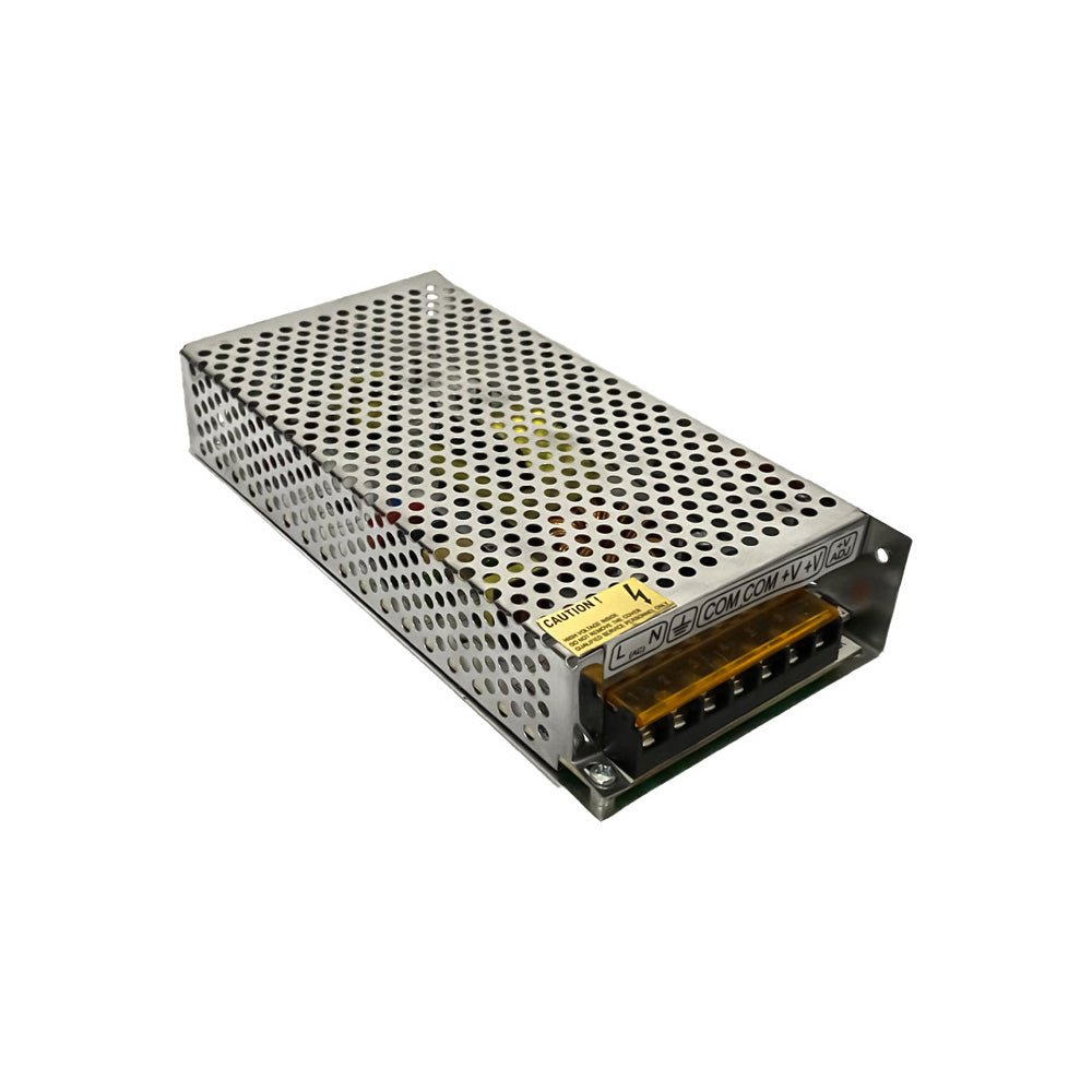
For a B2B buyer, a compliance logo alone does not show how a power supply will behave inside a different machine. Ask for the exact test report, configuration, cable arrangement, input range, load, enclosure, and product model. Confirm whether the report covers the intended product family standard and emission class. If the supply will operate beside servo drives, RF modules, sensors, or long field wiring, request integration guidance and a sample for system-level pre-compliance testing.
SIPURUI can support power supply selection around input range, load profile, enclosure, isolation, installation, and EMC integration requirements. Sharing the target standard and equipment wiring early gives the engineering team a better chance to recommend a suitable platform before the cabinet and cable architecture are fixed.
Conclusion
Switching power supply EMI begins with fast voltage and current transitions, but a compliance failure occurs only when energy finds a coupling path and an effective route to a measured port or antenna. That is why the most reliable workflow is to identify the noise mode, locate the physical source, trace the return path, and then choose the smallest effective change.
A compact hot loop, controlled switch-node area, engineered transformer capacitance, correctly rated safety capacitors, a damped filter, and repeatable pre-compliance testing usually deliver more than a late, oversized filter. EMI performance is a property of the complete electrical and mechanical system, not a single component.