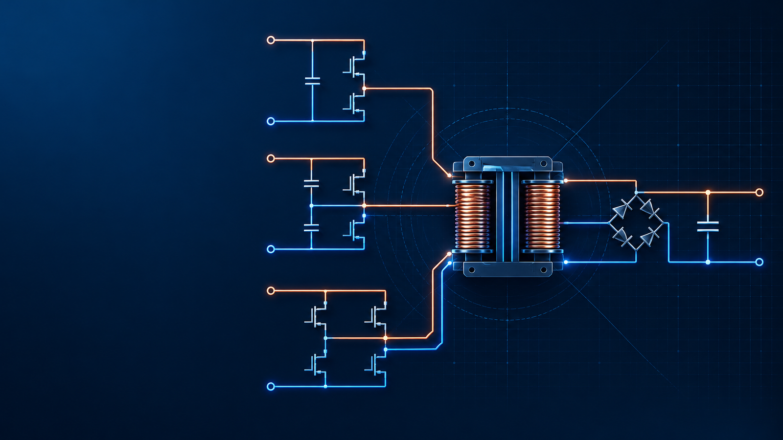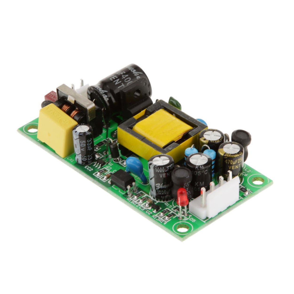
A switching converter can look perfectly reasonable on a schematic and still ring, overheat, fail EMC testing, or lose regulation on the first PCB. The difference is rarely mysterious. Fast current edges flow through real copper, vias, component leads, and capacitor connections. Those structures have resistance, inductance, and capacitance that the schematic does not show.
Good layout starts by asking where current changes fastest, where voltage changes fastest, and what reference the controller actually sees. That leads to three related jobs: keep commutation loops compact, protect low-level signals, and give every current a deliberate return path. This guide shows how to do that without relying on rules that break as soon as the topology, stack-up, or controller changes.
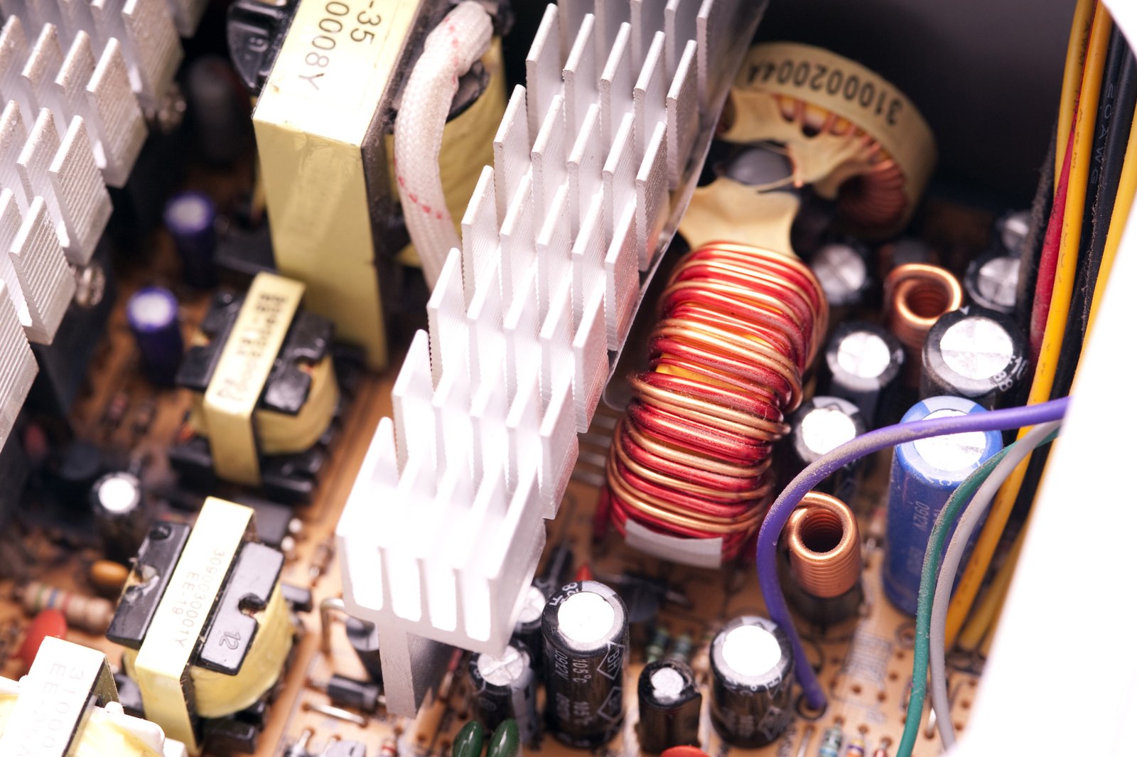
Why layout changes electrical behavior
The switching frequency printed in a data sheet is not the highest frequency that matters. A 300 kHz converter may have MOSFET edges lasting only a few nanoseconds. Those edges contain energy far above the fundamental switching frequency, which is why a few millimeters of shared return path or an oversized switch-node island can change conducted and radiated emissions.
Two relationships explain many failures:
A fast current change across parasitic inductance creates voltage error: V = L \cdot di/dt.
A fast voltage change drives displacement current through parasitic capacitance: I = C \cdot dv/dt.
The first produces overshoot, ground bounce, and gate ringing. The second couples switch-node noise into heatsinks, shields, adjacent copper, transformer windings, and feedback traces. Layout work is largely the process of controlling those unintended elements.
Start with the hot loop, not the board outline
The critical loop is the path whose current changes abruptly when the switch changes state. It is often called the hot loop or commutation loop. It is not necessarily the complete path that carries load current, and it is not always obvious from the simplified schematic.
For a synchronous buck converter, the highest-di/dt loop normally runs through the local input ceramic capacitor, high-side switch, low-side switch, and back to that capacitor. The inductor carries continuous current and sits outside this smallest commutation loop. For a nonsynchronous buck, the catch diode replaces the low-side MOSFET.
For a boost converter, pay particular attention to the pulsed path through the switch, rectifier, output capacitor, and their return connections. The inductor current is continuous, while the diode and output-capacitor current is discontinuous. For a flyback converter, there are two fast loops: the primary loop around the local bulk/high-frequency capacitor, transformer primary, and MOSFET; and the secondary rectifier loop around the transformer secondary, diode or synchronous rectifier, and output capacitor.
Place in current-flow order
Place the components that form each fast loop before routing feedback or auxiliary functions. The high-frequency ceramic capacitor must connect directly across the switching stage with a short, wide path. A nearby bulk electrolytic helps at lower frequencies but does not compensate for inductance between the ceramic capacitor and the switches.
Keep both the forward and return paths close. A short top-layer trace with a distant return on another part of the plane still makes a large loop. On multilayer boards, an adjacent reference plane or a tightly coupled vertical loop can reduce loop inductance. Use multiple vias when high transient current must change layers, and place those vias at the component pads rather than at the end of a copper extension.
| Topology | Fast loop to inspect first | Placement priority | Frequent mistake |
|---|---|---|---|
| Synchronous buck | Input ceramic capacitor, high-side MOSFET, low-side MOSFET | Put the ceramic capacitor directly beside the half bridge | Treating the inductor and bulk capacitor as the whole hot loop |
| Nonsynchronous buck | Input ceramic capacitor, switch, catch diode | Minimize the capacitor-switch-diode polygon | Long diode return to a general ground pour |
| Boost | Switch, rectifier, output capacitor, local return | Keep diode and output capacitor close to the switching stage | Optimizing only the input path because input current is large |
| Flyback primary | Local bus capacitor, primary winding, MOSFET | Cluster the three and reserve space for clamp/snubber | Routing the MOSFET return through a shared controller ground path |
| Flyback secondary | Secondary winding, rectifier, output capacitor | Make the rectifier loop compact and wide | Putting the output capacitor near the connector instead of the rectifier |

Treat the switch node as an antenna
The switch node has high dv/dt. It needs enough copper for current and heat, but unnecessary area adds electric-field coupling. Use a short, wide connection between the switch and inductor or transformer, avoid branches and test-point stubs, and do not run feedback, current-sense, enable, or clock traces beside or underneath it.
The right copper area is a tradeoff. Shrinking it with a narrow neck raises resistance and inductance; flooding it across the board increases capacitive coupling and radiation. Start from the controller vendor's evaluated layout, keep the electrical connection compact, and add thermal copper where it does not enlarge the noisy node indiscriminately.
Do not assume that every layer must be voided below an inductor or switch node. A keepout under a high-dv/dt node can reduce capacitive coupling, but an intact ground plane can improve shielding and return continuity elsewhere. The decision depends on the component construction, layer spacing, safety requirements, and EMC target. Document the chosen keepouts so a later copper-pour update does not silently remove them.
Route power paths for current and heat
Trace width cannot be selected from a universal “mils per amp” rule. Copper thickness, external versus internal layers, allowable temperature rise, ambient temperature, nearby copper, via count, and pulse duration all matter. Size conductors with an accepted current-capacity method such as IPC-2152 guidance or validated field-solver/thermal results, then confirm the hottest operating condition on hardware.
Avoid neck-downs at pads, fuses, connectors, and layer transitions. When current changes layers, use a via array with sensible spacing and enough annular copper. For power packages with exposed pads, follow the data-sheet thermal-via pattern; filling the area with random small vias can create assembly problems without delivering the expected thermal path.
Thermal layout also affects electrical performance. Hot electrolytic capacitors lose life, hot magnetics change loss, and MOSFET R_{DS(on)} rises with junction temperature. Keep heat-producing components away from temperature-sensitive references and feedback dividers. Leave airflow and enclosure orientation in the review, because a board that is comfortable on an open bench may run much hotter when mounted vertically inside a sealed cabinet.
Give sensitive signals their own quiet neighborhood
Feedback, compensation, current sense, oscillator, soft-start, and enable pins work with small signals. Group their components around the controller, away from the switch node, gate-drive loop, magnetics, and rectifier connections.
Use Kelvin sensing where the voltage matters
Take output-voltage feedback from the point being regulated, normally at the output capacitor or designated remote-sense point. Route the sense and its reference as a pair where practical. Do not let load current share either connection between the sense point and controller input. For a shunt or current-sense resistor, route separate Kelvin traces from the resistor pads; connecting somewhere along the high-current copper includes unknown copper drop in the measurement.
Place the feedback divider and compensation network close to the IC. The high-impedance feedback node should be physically small. If the data sheet recommends a feed-forward or filtering capacitor, place it at the relevant pins and use the specified reference ground. Avoid casually adding capacitance: it can alter loop response or current-limit timing.
Keep gate-drive loops local
The gate driver, gate resistor, MOSFET gate, and source-return connection form another high-di/dt loop. Keep it short and separate from power-current return paths. A dedicated Kelvin source pin should return directly to the driver when the package provides one. Route gate and return together; equal geometric length is less important than low loop inductance and a clean source reference.
Decouple at the pins
Place controller and driver bypass capacitors at their supply and return pins. The connection should be a compact loop, with no via or narrow trace shared with noisy switching current if the package and stack-up allow it. Use the values and placement guidance in the controller data sheet rather than assuming that one 0.1 µF capacitor covers every device and frequency range.
| Sensitive network | Preferred connection | Keep away from | Lab symptom when compromised |
|---|---|---|---|
| Output feedback | Kelvin pair from the output capacitor or remote-sense point | Switch node, inductor hot end, gate traces | Output jitter, load-dependent setpoint error |
| Current sense | Separate traces from sense-element pads | Commutation loop and shared high-current copper | False current limit, subharmonic behavior, pulse skipping |
| Compensation | Components tight to controller pins and analog reference | Magnetic components and fast edges | Low-frequency oscillation or poor transient recovery |
| Gate drive | Short gate-and-return loop, Kelvin source when available | Sense and feedback paths | Gate ringing, false turn-on, excess switching loss |
| Enable/soft-start | Short trace, defined impedance, local filtering if specified | Connectors and long exposed board edges | Random startup, hiccup operation, nuisance shutdown |
Grounding: design return paths, not labels
“Ground” is a set of current paths, not a perfect zero-volt reservoir. The objective is to prevent noisy power current from flowing through the copper used as the controller's measurement reference.
Some controllers expose AGND and PGND pins and specify where they join. Others are designed for a solid ground plane with local partitioning and careful placement. Follow that architecture. A blanket rule to split every ground and join it at one star point can force return current around slots, increasing loop area and EMI. Conversely, connecting a sensitive reference anywhere on a busy power plane can inject switching voltage into the control loop.
A useful approach is to identify each return current, mark its source and destination, and keep high-current switching returns local. Join analog and power references at the point specified in the controller data sheet, often near the IC exposed pad, low-side source, or a local capacitor terminal. Never route a signal across a split in its reference plane; the return current will take a detour or couple through unintended capacitance.
Protective earth is not signal ground
Protective earth (PE), chassis/frame ground, primary DC bus return, and SELV output return have different jobs. PE connections must satisfy safety and fault-current requirements. Chassis bonding and Y-capacitor placement affect common-mode EMI, but any connection across an isolation barrier must use safety-rated parts and respect leakage-current limits.
In an isolated flyback supply, primary and secondary copper must maintain the required clearance and creepage. Those distances are not universal. Working voltage, transient overvoltage category, pollution degree, material group, altitude, coating, insulation system, and the applicable product standard all change the requirement. Use the relevant safety standard and certification plan; do not copy a spacing value from an unrelated board.
Topology-specific review points
Buck converter
First inspect the input ceramic capacitor and half-bridge loop. Next, check switch-node area, gate-drive return, and the connection from the output capacitor to the regulated load. The feedback pickup should be on the quiet side of the output capacitor, away from the inductor's switch-node end. In a multiphase design, symmetry matters, but identical trace length should not come at the cost of larger commutation loops.
Boost converter
The input inductor current is continuous, but the diode and output-capacitor current is pulsed. Keep the switch, diode, and output capacitor compact, and make the switch node small. Kelvin-route current sense and feedback. If the controller uses slope compensation or a sensitive current-sense pin, follow its reference layout closely.
Isolated flyback converter
Separate primary and secondary floor plans before placement becomes crowded. Keep the primary and secondary commutation loops compact on their respective sides. Place the clamp or snubber next to the elements it serves; a snubber at the end of a long trace cannot control the local ringing well. Keep optocoupler/secondary feedback components away from transformer switching nodes, and preserve the isolation boundary through every copper layer, via, mounting hole, and heatsink feature.
A practical layout review sequence
Print the top and bottom copper at a scale large enough to mark by hand, or use colored overlays in the CAD tool. Review in this order:
1. Draw every high-di/dt loop for each switching state. Confirm that the local capacitor closes the loop.
2. Highlight every high-dv/dt node and inspect copper on all layers above and below it.
3. Trace feedback and current-sense paths from the physical sense point to the controller, including their returns.
4. Check gate-drive loops, bypass capacitors, and layer transitions.
5. Verify current density, neck-downs, via arrays, thermal paths, and connector ratings.
6. Audit isolation, creepage, clearance, slots, mounting hardware, and chassis connections against the product standard.
7. Compare the board with the controller evaluation module and data-sheet layout. Any difference should have a reason.
| Symptom during bring-up | Layout-related suspects | What to measure first | Typical correction |
|---|---|---|---|
| MOSFET overshoot or failure | Large commutation loop, long source return, poor probe setup | VDS with a low-inductance probe connection | Re-place local capacitor/switches; shorten forward and return paths; tune clamp/snubber after layout is sound |
| Audible noise or pulse jitter | Noisy feedback/current sense, unstable operating mode, magnetic movement | Switch-node timing and feedback ripple across load range | Kelvin-route sensing; separate it from noisy nodes; confirm compensation and operating mode |
| Excess output ripple | Shared feedback return, poor output-capacitor connection, probing loop | Ripple directly at capacitor with a spring ground | Correct sense/return point; reduce rectifier-loop impedance |
| High temperature | Copper bottleneck, inadequate vias, excess ringing or slow gate transition | Loss split and thermal image after stabilization | Fix current path and thermal spreading; then adjust gate resistance if required |
| EMC failure | Large hot loop, excessive switch-node area, common-mode coupling | Near-field scan and LISN spectrum correlated with switch edges | Reduce loop/node area, restore return continuity, optimize filtering and chassis path |
Prototype validation that reveals layout faults
Use measurement technique that does not create the problem. A long oscilloscope ground lead can show ringing that is mostly in the probe loop. Use a ground spring, coax pigtail, differential probe, or a properly designed measurement connector as appropriate to the voltage and safety category.
Test at minimum and maximum input, light load, full load, startup, shutdown, short-circuit recovery, and the thermal worst case. Correlate switch-node and gate waveforms with output behavior. A near-field probe is useful for locating radiating loops before formal EMC testing. Thermal imaging can expose a trace neck-down, a saturated magnetic component, or switching loss that average efficiency data hides.
Layout checklist for design release
The high-frequency loops are identified from switching-state current paths, not guessed from total load current.
Local ceramic capacitors close the commutation loops with short forward and return connections.
Switch-node copper is compact, free of stubs, and separated from sensitive networks.
Feedback and current sense use deliberate Kelvin connections and clean references.
Gate-drive and bypass loops are local and do not share noisy return impedance.
Current paths have no hidden bottlenecks at pads, vias, connectors, or fuses.
Ground strategy matches the controller architecture; signal returns do not cross plane splits.
Primary/secondary separation and PE/chassis connections meet the applicable safety plan.
Thermal behavior has been checked in the real enclosure and mounting orientation.
Probe points allow safe, low-inductance measurement without adding large stubs to fast nodes.
Conclusion
A reliable power PCB is built around current paths and electric fields. Compact commutation loops reduce inductive overshoot. Controlled switch-node copper reduces capacitive coupling. Kelvin-routed sensing and intentional return paths keep the controller referenced to the voltage it is supposed to regulate.
The most useful review question is simple: where does this current return during each switching state? If the answer requires crossing a split, sharing a sensitive trace, or traveling to a distant capacitor, the layout still needs work.
SIPURUI works with industrial power-supply customers on designs intended for demanding equipment and control environments. When comparing a standard or custom supply, ask for evidence from thermal, protection, and EMC testing, and review how the PCB layout supports those results.