A switching power supply can pass basic output-voltage checks and still fail under load steps, light-load operation, or wide input conditions. This guide explains how topology selection, loop compensation, and stability testing work together in practical industrial power supply design.
Start with topology, not component values
A power supply can look correct on paper and still misbehave on the bench. The output rings after a load step. A prototype oscillates only at half load. A capacitor change that should reduce ripple makes the waveform worse. These are not rare surprises. They are usually signs that topology choice, loop compensation, and stability testing were treated as separate tasks when they actually live in the same control problem.
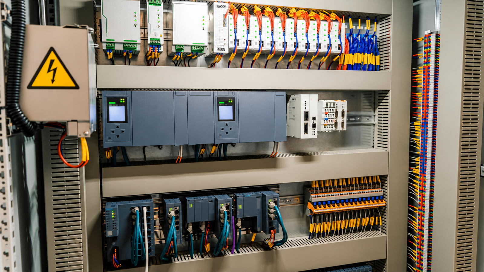
For industrial equipment, that problem is more than an engineering inconvenience. A marginally stable supply can reset a PLC, disturb a sensor rail, shorten capacitor life, or fail EMC testing late in the project. It can also create an uncomfortable purchasing issue: the first samples pass, but field units fail when cable length, enclosure temperature, or input voltage changes.
This guide turns the usual theory into a practical design sequence. It is written for hardware engineers, automation integrators, equipment manufacturers, and technical buyers who need to judge whether a switching power supply design has enough margin for real operating conditions.
Topology selection decides the basic stress profile of the supply. It affects switch voltage, diode current, transformer design, output ripple, EMI behavior, isolation, cost, and how difficult the control loop will be to stabilize. If the topology is wrong for the input and load profile, compensation becomes repair work rather than design work.
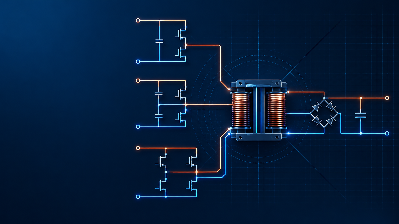
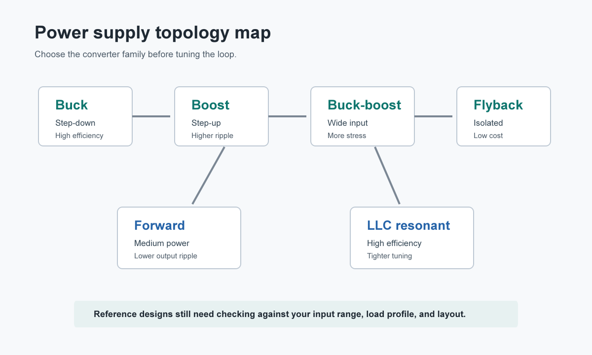
The first question is the voltage relationship. If the input is always higher than the output, a buck converter is usually the cleanest answer. If the output must sit above the input, a boost converter fits. If the input can move above and below the output set point, buck-boost, SEPIC, or a related non-inverting structure may be required. When safety isolation or noise separation matters, the discussion moves toward flyback, forward, active-clamp forward, LLC, or other isolated converters.
Power level narrows the choice quickly. Flyback converters remain attractive for adapters, auxiliary supplies, standby rails, and many low-to-medium power isolated outputs because they keep the magnetic structure simple. At higher power, a forward or resonant topology often gives better transformer utilization, lower current stress, and improved efficiency. That improvement comes with design overhead: reset circuits, synchronous rectification timing, resonant tank tolerance, or more demanding controller setup.
| Topology | Input-output relationship | Typical B2B use | Main advantage | Common limitation |
|---|---|---|---|---|
| Buck | Step-down | Control boards, 24 V to logic rails, battery systems | High efficiency and simple power stage | Cannot boost when input drops below output |
| Boost | Step-up | LED drivers, backup rails, battery boost stages | Simple way to raise voltage | Higher output ripple and no output disconnect in many designs |
| Buck-boost / SEPIC | Step-up or step-down | Wide input equipment, automotive-like rails, battery charge paths | Handles input crossing the output set point | More components and higher stress than a buck |
| Flyback | Isolated step-up or step-down | Adapters, auxiliary supplies, small industrial modules | Low cost isolation with multiple outputs possible | Transformer leakage, EMI, and power scaling limits |
| Forward / active clamp | Isolated step-down | Higher power isolated DC rails | Lower ripple and better power handling than many flybacks | Needs reset or clamp design and tighter magnetic control |
| LLC resonant | Isolated high-efficiency conversion | Compact AC-DC and high-efficiency industrial supplies | High efficiency at suitable load range | Harder to tune across light load and wide input |
The common mistake is copying a reference design because the output voltage and current look similar. A reference design is useful, but it reflects a specific input range, PCB layout, magnetic part, capacitor mix, controller mode, and intended load behavior. Change enough of those conditions and the loop can move into a very different place.
How topology changes the control problem
Every topology gives the compensator a different plant to control. A voltage-mode buck converter with an LC output filter has a double pole that needs compensation support. A boost or flyback operating in continuous conduction mode introduces a right-half-plane zero, which limits how high the crossover frequency can be pushed. A converter that moves between continuous and discontinuous conduction mode can change loop gain across load conditions.
That is why a supply may behave well at full load and ring at light load, or pass at nominal input and oscillate at low line. The problem is not always a bad capacitor or a poor controller. Sometimes the selected topology leaves too little control margin for the required input and output window.
For B2B equipment, the load profile matters as much as the nameplate wattage. A motor-control cabinet may draw short current bursts. A communication device may spend most of its life at light load and then wake quickly. A sensor system may need very low ripple more than peak efficiency. These details should influence topology choice before layout begins.
Loop compensation makes the supply behave
A regulated switching power supply is a feedback system. The output is sensed, compared with a reference, processed by an error amplifier or digital controller, and converted into PWM or switching-frequency decisions. Compensation shapes that feedback path so the converter responds quickly enough without turning the LC filter, output capacitors, parasitics, and load into an oscillator.
In simple terms, compensation answers two bench-level questions. How fast should the supply react when the load changes? How much stability margin remains when it reacts that fast?
Engineers usually look at three indicators:
| Indicator | Practical target | What it tells you |
|---|---|---|
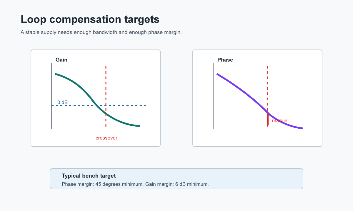
| Phase margin | 45 degrees minimum, 60 degrees or more preferred for many industrial designs | How much phase delay the loop can tolerate before oscillation risk becomes high |
| Gain margin | 6 dB minimum, 10 dB or more preferred | How much gain increase the loop can tolerate near the critical phase point |
| Crossover frequency | Often around 1/10 to 1/20 of switching frequency, subject to topology and noise limits | How fast the loop responds to disturbances |
These targets are guidelines, not guarantees. A boost or flyback with a right-half-plane zero may need a lower crossover frequency. A second-stage LC filter after the main output can add phase delay and reduce margin. Long remote-sense wiring can also make the loop see a different output node than the load actually experiences.
Most analog designs use Type I, Type II, or Type III compensation. Type I is simple and slow. It may work for lightly stressed rails where transient response is not demanding. Type II compensation is common in current-mode supplies and many practical industrial designs. Type III compensation adds more shaping ability and often appears in voltage-mode buck designs or tighter transient applications.
The familiar pole-zero equations still matter:
| Compensation element | Basic equation | Design use |
|---|---|---|
| Zero frequency | fz = 1 / (2 pi Rz Cz) | Adds phase boost near the power-stage double pole or desired crossover region |
| Pole frequency | fp = 1 / (2 pi Rz Cp) | Rolls off high-frequency gain to reduce noise sensitivity |
| Crossover planning | fc often sits below switching-frequency-related noise and topology limits | Balances transient speed against margin |
The lab result matters more than the spreadsheet. Capacitor ESR, ceramic capacitance loss under bias, optocoupler variation, transformer leakage, injection resistor choice, and PCB parasitics all move the real loop away from the clean calculation.

A practical compensation workflow
Start by defining the worst cases. Minimum input, maximum input, light load, full load, hot enclosure, cold start, and the fastest expected load step should all be on the list. Do not tune the loop only at nominal input and room temperature unless the product will only live there, which industrial hardware rarely does.
Next, estimate the power-stage behavior and set a realistic crossover target. For a buck converter, the output LC filter and ESR zero drive much of the compensation design. For a flyback, transformer leakage, optocoupler response, output capacitor ESR, and operating mode deserve attention. If the controller vendor provides a small-signal model or design tool, use it, then assume the bench will still have the final vote.
After the first compensation values are selected, measure. A frequency response analyzer, or an oscilloscope with frequency response analysis, can inject a small signal into the feedback path and produce a Bode plot. The injection point must be chosen carefully so the loop remains closed for DC regulation while the AC perturbation reveals loop gain and phase.
Then check time-domain behavior. A load step should show controlled undershoot or overshoot, acceptable settling time, and no long ringing tail. If the waveform rings at a frequency close to a Bode plot concern, the evidence is pointing in the same direction. That is much more useful than adjusting capacitors by feel.
Stability analysis: what to test before release
Stability testing should combine time-domain and frequency-domain evidence. A clean ripple waveform is useful, but it does not prove loop margin. A good Bode plot is valuable, but it does not replace load-step and start-up behavior under real cable, load, and temperature conditions.
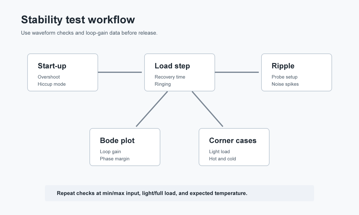
The release test plan should include at least:
| Test | What to watch | Common warning sign |
|---|---|---|
| Start-up at min and max input | Overshoot, hiccup, monotonic rise, interaction with load | Repeated restart or output ringing during soft start |
| Load step at several operating points | Voltage dip, overshoot, recovery time, ringing | Underdamped ringing that changes sharply with load |
| Ripple and noise | Probe grounding, bandwidth limit, load condition | High-frequency spikes caused by layout or poor probing technique |
| Bode plot | Crossover, phase margin, gain margin | Low phase margin, multiple crossover points, unexpected gain peaking |
| Light-load and no-load operation | Mode transition, burst behavior, audible noise | Low-frequency oscillation or unstable burst packets |
| Temperature check | Capacitance shift, optocoupler CTR, semiconductor behavior | Stable at room temperature but marginal when hot or cold |
One practical note: do not ignore light load. Many industrial products now have standby power targets or spend long periods waiting for a command. At light load, controllers may enter pulse skipping, burst mode, or discontinuous conduction. The loop gain changes, audible noise can appear, and output ripple may look very different from the full-load waveform.
Troubleshooting unstable behavior
When a supply oscillates, first identify the frequency and operating condition. Low-frequency oscillation often points toward loop bandwidth, compensation placement, optocoupler behavior, or mode transition. High-frequency ringing is more often tied to layout parasitics, switch-node coupling, diode recovery, transformer leakage, or inadequate local decoupling.
| Symptom | Likely area to investigate | Practical next step |
|---|---|---|
| Low-frequency oscillation below about 10 kHz | Loop compensation, optocoupler pole, light-load mode | Measure Bode plot and compare margin at the failing load point |
| Ringing after load step | Low phase margin or output filter resonance | Adjust zero/pole placement and check output capacitor ESR mix |
| High-frequency spikes above 100 kHz | PCB layout, switch-node coupling, snubber design, probe method | Shorten high di/dt loops and verify with a low-inductance probe setup |
| Stable full load but unstable light load | CCM/DCM transition, burst mode, insufficient preload | Test controller mode settings or add a carefully sized preload if acceptable |
| Start-up hiccup or repeated restart | Soft-start timing, current limit, transformer saturation, output capacitance | Check inrush, current-limit waveform, and bias supply behavior |
| Worse ripple after capacitor substitution | ESR or capacitance shift changed loop zero | Recalculate output filter behavior and remeasure loop margin |
The capacitor example is common. Replacing an electrolytic capacitor with a ceramic array may reduce ESR so much that the original ESR zero disappears. The ripple measurement may look worse, or the loop may lose phase boost near crossover. Lower impedance is not automatically better when the compensator was designed around the old output network.
PCB layout can undo good math
Control loops do not live in schematics. They live on copper.
Keep high di/dt paths short: the input capacitor, switch, diode or synchronous FET, and transformer or inductor loop must be tight. Separate noisy switch nodes from feedback traces. Place compensation components close to the controller pins. Route remote sense as a quiet pair when used, and avoid letting power current share the same return path as the feedback reference.
Grounding deserves a calm, deliberate review. A small voltage error in the sense ground can look like output ripple to the controller. The controller then corrects an error that the load may not actually see. That is one reason bench waveforms sometimes improve when the probe ground changes. The measurement setup was part of the circuit.
What buyers and integrators should ask suppliers
Technical buyers do not need to redesign the supply, but they should ask for evidence that the design has margin. For custom or semi-custom industrial power supplies, request operating range test data, load transient results, thermal derating information, and any available loop-stability measurements. If the supplier cannot share a Bode plot, they should still be able to explain how stability was verified across input, load, and temperature.
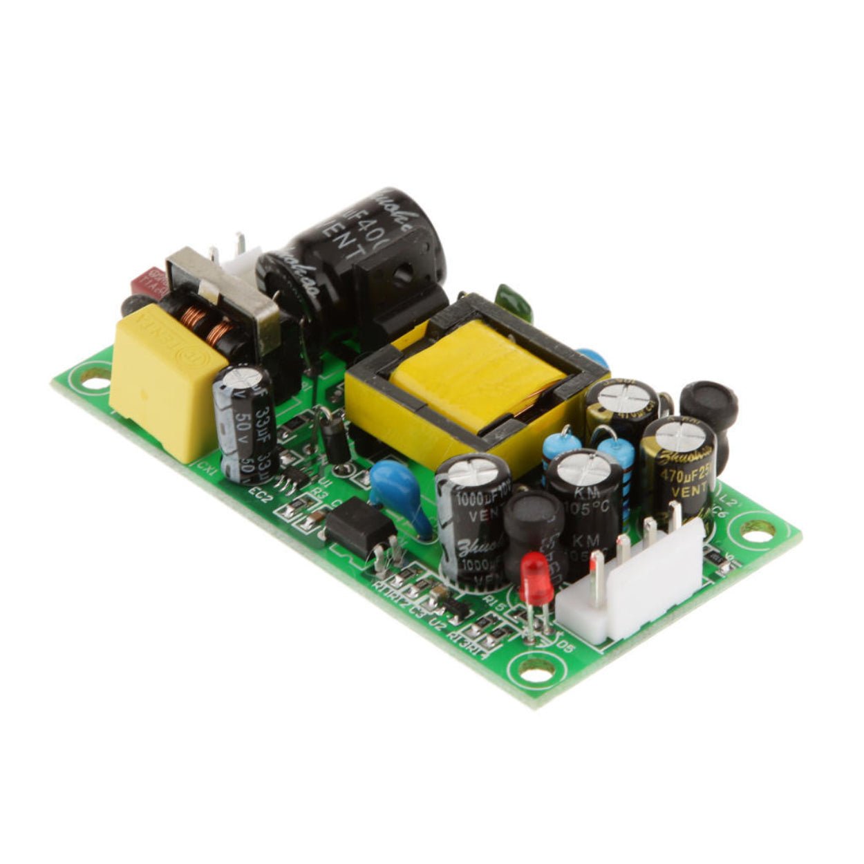
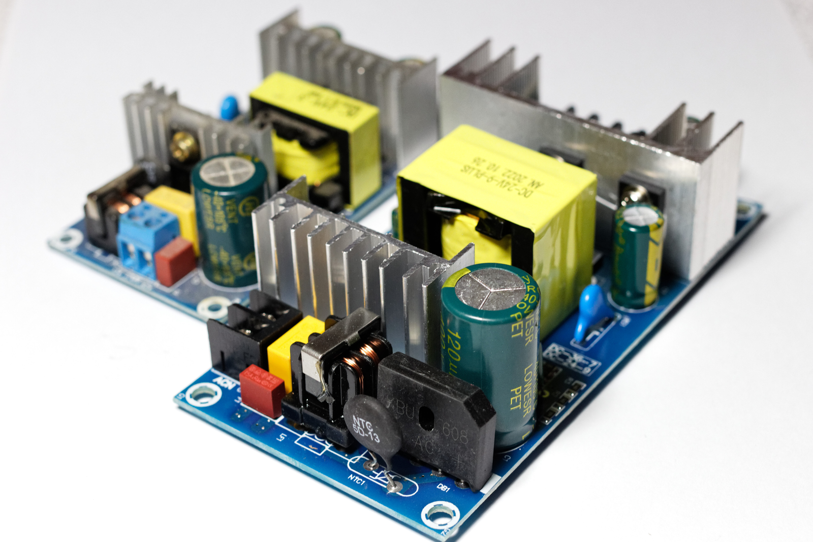
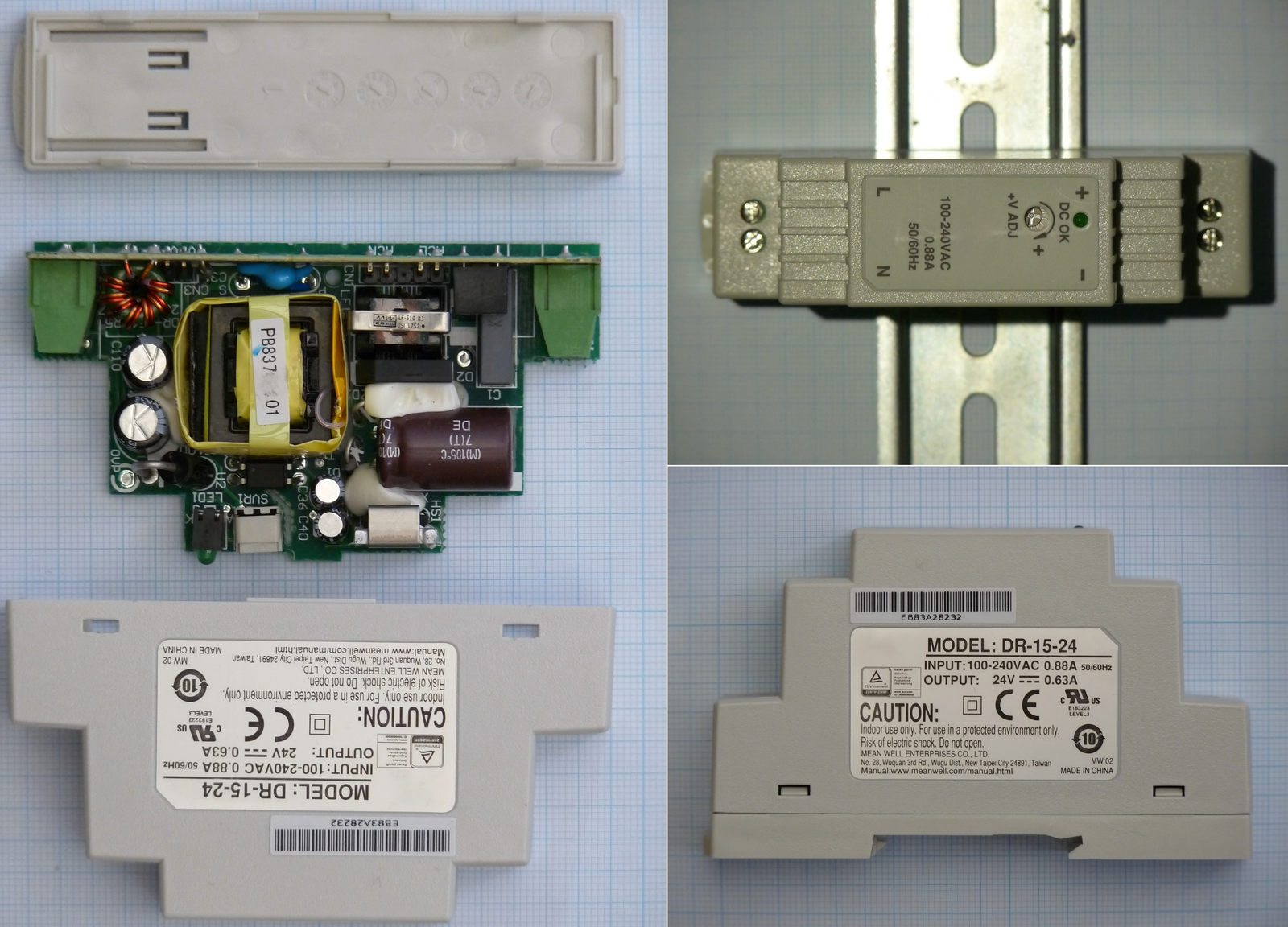
For a DIN-rail supply, enclosed AC-DC module, or open-frame embedded unit, ask how the product behaves with long output wiring, pulsed loads, parallel capacitive loads, and light-load standby operation. Those are the situations that often expose marginal stability after installation.
Conclusion
Topology selection, loop compensation, and stability analysis are not three separate boxes to tick. Topology defines the control problem. Compensation shapes the loop. Stability testing proves whether the design has enough margin outside nominal conditions.
For engineers, the best habit is to connect calculations with measurement early. For equipment manufacturers and buyers, the best habit is to ask for evidence before the supply becomes a field problem. SIPURUI works with industrial switching power supply applications where reliability, installation environment, and real load behavior matter; the right technical discussion at the selection stage usually saves time during commissioning.
Buyer Checklist
- Confirm topology against input range, output voltage, isolation needs and load profile.
- Review crossover frequency, phase margin and gain margin before approving samples.
- Test start-up, load step, ripple, light-load behavior and temperature corners.
- Ask suppliers for transient, thermal derating and stability evidence for the intended installation.