A practical workflow for diagnosing conducted and radiated EMI in switching power supplies by identifying the failing frequency, separating differential-mode and common-mode current, tracing return paths, and verifying each fix.
Overview
A switching power supply can regulate correctly, meet its efficiency target, survive thermal testing, and still fail EMC at the end of development. That failure often triggers a familiar reaction: add a larger X capacitor, try another common-mode choke, clip ferrites onto every cable, and hope the next scan is better.
That approach sometimes moves a peak, but it rarely builds a repeatable fix. EMI work becomes much faster when the team treats the test result as evidence. First identify the failing frequency and operating condition. Then determine whether the dominant current is differential mode (DM) or common mode (CM), trace its return path, and change one variable at a time.
This guide explains that workflow for AC/DC switching power supplies and related industrial power converters. It also points out where common rules of thumb break down.
Start with the failing test, not a parts list
Conducted and radiated emissions describe how unwanted RF energy reaches the measurement system. They are not two unrelated design defects.
Conducted emissions are measured on cables through a defined impedance network, commonly a LISN on the power input. Many product standards evaluate mains-port emissions from 150 kHz to 30 MHz, although the exact range and detector settings depend on the applicable standard.
Radiated emissions are measured with an antenna or, in some product standards, by current-probe or absorber-clamp methods. A common radiated range begins at 30 MHz, but the upper frequency and test distance vary with the product and standard.
The same switching edge can contribute to both. A drain-voltage transition may capacitively drive common-mode current through transformer interwinding capacitance. Part of that current appears at the LISN; another part flows onto an output cable and makes the cable radiate. A narrow focus on the label “conducted” or “radiated” can therefore hide the shared source.
Before changing hardware, record five items: the applicable limit, the failing frequencies and margin, detector type, operating state, and test configuration. Photographs of cable routing and grounding are valuable. A fix that only works with a cable folded differently is not production-ready.
| Evidence from the scan | Likely starting hypothesis | Fast confirmation method |
|---|---|---|
| Peaks at switching frequency and low-order harmonics | DM ripple current or input-filter weakness | DM/CM separator, two-channel LISN math, or current probe on individual conductors |
| Broadband rise or ringing-related peaks | Fast edge exciting parasitic L-C network | Oscilloscope with a short ground spring; compare ring frequency with scan |
| Large change when both conductors pass through one clamp | CM current on the cable | Clamp both conductors together so DM flux cancels |
| Peak changes strongly with cable position | Cable is an efficient radiator or return path | Repeat with controlled cable geometry and add a temporary common-mode ferrite |
| Peak responds to a near-field probe over the switch node | Local electric-field source | Reduce switch-node copper or add a temporary grounded shield for diagnosis |
Differential mode and common mode are current paths
DM current flows out on one conductor and returns on the other. In an AC input, the line and neutral noise currents are opposite in direction. Pulsed converter input current, diode commutation, and the impedance of the bulk and high-frequency capacitors often set the DM signature.
CM current flows in the same direction on the power conductors and returns through chassis, protective earth, a reference plane, parasitic capacitance, the load, or the measurement environment. In isolated converters, transformer interwinding capacitance and capacitance from the primary switch node to a heatsink or enclosure are frequent coupling paths.
Frequency alone does not prove the mode. DM often dominates near the switching fundamental, while CM is frequently important at higher harmonics, but either mode can appear across a wide range. Measure or deliberately perturb the suspected path before committing to a filter redesign.

Find the source, coupling path, and antenna
An emissions problem needs all three. The source is usually a high di/dt current loop or high dv/dt node. The coupling path can be intentional copper, transformer capacitance, heatsink capacitance, a poorly bonded enclosure, or a cable. The antenna may be a large PCB loop, a heatsink, or an external harness.
The highest-value PCB change is usually to shrink the hot loop. Place the switching device, rectifier or synchronous device, and high-frequency input capacitor so the commutating current path is short and compact. Keep the switch-node copper no larger than necessary. Route gate-drive and current-sense returns so they do not share inductance with power current.
For an isolated flyback or forward converter, inspect both primary and secondary commutation loops. A quiet primary does not compensate for a long secondary rectifier-to-capacitor loop. Transformer construction also matters: winding order, shields, and interwinding capacitance can change CM current substantially.
Snubbers are useful when a measured ringing mode creates a failing peak. Measure the ringing frequency, estimate the parasitic network, and tune the RC or RCD network. Oversizing a snubber wastes power and raises temperature; using one without confirming the responsible resonance can simply trade one peak for another.
A disciplined conducted-emissions workflow
1. Reproduce the failure on a controlled bench
Use the specified LISN, ground plane, cable lengths, load, and operating mode as closely as possible. Preserve the compliance-lab cable arrangement. Pre-compliance results are most useful when their relative changes track the formal setup, even if absolute amplitudes differ slightly.
2. Separate DM from CM
A DM/CM separator is ideal. Without one, compare currents with a clamp around one conductor and then around both line and neutral. Passing both through the probe cancels the opposing DM flux and reveals the residual CM current. For offline equipment, use safe, appropriately rated probes and fixtures.
3. Treat the source before increasing the filter
Check the switch-node ringing, diode reverse recovery, gate resistance, transformer leakage inductance, and placement of the high-frequency bypass capacitor. A small source reduction can remove several filter stages later. Slowing the gate edge can help, but confirm switching loss, device stress, dead time, and thermal margin at minimum and maximum input voltage.
4. Size the filter for the measured attenuation gap
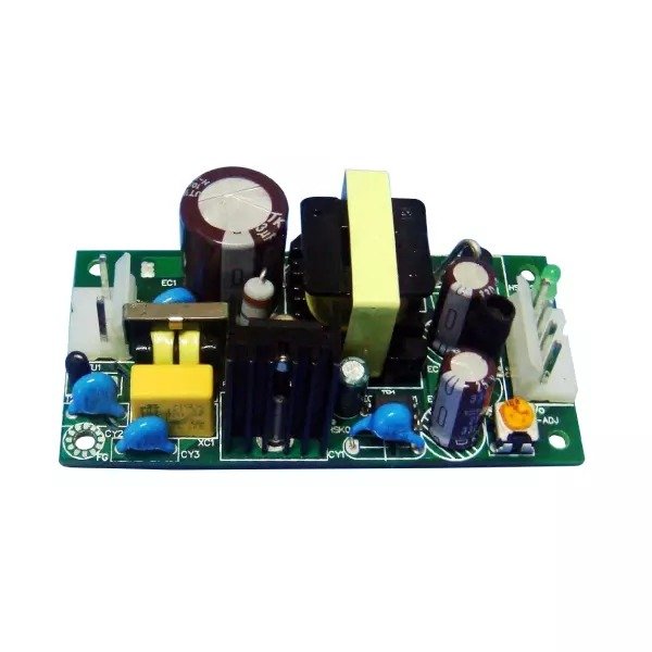
An X capacitor and differential inductor form a DM low-pass network. A common-mode choke provides impedance to in-phase cable current, while Y capacitors provide a controlled high-frequency return path. Their real behavior includes ESR, ESL, winding capacitance, leakage inductance, and self-resonance. More capacitance or inductance does not guarantee more attenuation at the failing frequency.
Place the filter at the cable entry and keep its dirty side physically separated from its clean side. If an input trace runs around the choke and couples back to the converter side, the noise can bypass the filter through electric or magnetic fields.
5. Check interaction, safety, and damping
An input filter can interact with a converter’s negative incremental input impedance. Review control-loop stability or use the converter vendor’s input-filter criteria. Confirm inrush current, X-capacitor discharge time, choke saturation and temperature, capacitor ripple rating, and abnormal-operation behavior.
Y-capacitor changes need particular care. The allowable capacitance depends on insulation class, accessible metal, protective-earth arrangement, touch-current limits, and the applicable safety standard. In Class II supplies, a Y capacitor may connect primary to secondary rather than line to chassis. Never choose its value from an EMI plot alone.
Fixing radiated emissions without chasing random peaks
Below roughly a few hundred megahertz, attached cables often dominate because they are electrically long enough to radiate CM current efficiently. At higher frequencies, local PCB structures, package transitions, heatsinks, seams, and short cable sections can become effective radiators. This is a diagnostic tendency, not a fixed boundary.
Start with a current probe on each external cable. If a temporary clamp ferrite around the entire cable bundle reduces the chamber peak, the cable current is part of the problem. Then find how that current reaches the cable: transformer capacitance, a connector ground discontinuity, an unbalanced output filter, or a noisy reference plane.
Near-field E- and H-field probes help localize board-level sources. An H-field probe is useful around hot loops and magnetic components; an E-field probe responds strongly near high dv/dt copper. Probe readings are comparative rather than direct compliance measurements, so keep probe position and orientation consistent.
Cable and connector fixes
A clamp ferrite is an excellent diagnostic tool and can be a production fix if its impedance, current rating, temperature behavior, and installation are controlled. Routing the forward and return conductors together reduces loop area. For shielded cables, terminate the shield with a low-inductance 360-degree connection where practical; a long pigtail loses effectiveness quickly at high frequency.
PCB and component fixes
Reduce hot-loop area, shorten the switch node, improve high-frequency capacitor placement, and keep noisy copper away from board edges and connectors. A ferrite bead can help when its impedance peak overlaps the problem frequency and its DC bias and heating are acceptable. It is not a general replacement for a DM inductor or common-mode choke.
Enclosure and shield fixes
A shield works only when displacement current has a low-impedance return. At RF, a short, wide bond is usually better than a long “single-point” wire. Multiple enclosure bonds may be appropriate because they reduce inductance and seam impedance; the correct strategy depends on frequency, safety architecture, corrosion control, and whether low-frequency ground-loop current is a concern. Treat seams, apertures, display openings, and cable penetrations as part of the shield.
What each mitigation component can and cannot do
| Component or change | Best use | Design check that prevents a bad fix |
|---|---|---|
| X safety capacitor | DM attenuation across line and neutral | Inrush, discharge, reactive current, class and rated voltage |
| Differential inductor | DM impedance at lower-frequency harmonics | Saturation, copper loss, damping, converter input stability |
| Common-mode choke | CM impedance on a cable pair or bundle | Impedance curve under bias, winding capacitance, leakage inductance, temperature |
| Y safety capacitor | Controlled CM return path | Safety class, touch current, insulation system, production tolerance |
| Ferrite bead or clamp | Targeted RF loss at a known band | Impedance versus frequency and bias, heating, cable installation repeatability |
| RC/RCD snubber | Damping a measured resonance or leakage spike | Loss, device stress, temperature, component tolerance |
| Shield or chassis bond | Containing electric fields and returning RF current | Bond inductance, seams, apertures, coating, connector termination |
Change one variable and keep a margin ledger
EMI debugging deteriorates quickly when several parts are added at once. Use a change log with the failing frequency, original amplitude, modification, new amplitude, efficiency, temperature, and safety impact. Keep the analyzer settings and cable arrangement unchanged.
Temporary copper foil, clamp ferrites, small capacitors, removable shields, and alternate gate resistors are useful diagnostic tools. Once the sensitive path is known, redesign it into a controlled production solution. A ferrite balanced on a cable during a lab scan is evidence, not yet a manufacturing specification.
Verify beyond the passing scan
Repeat the test at minimum and maximum input voltage, light load, full load, and any burst, skip, standby, or fan-control modes. Some converters are quiet at rated load but create low-frequency clusters in burst mode. Others produce their strongest ringing at high line and light load.
Then verify the price of the fix: efficiency, no-load power, component temperature, inrush, transient response, control-loop stability, leakage or touch current, dielectric withstand, and abnormal operation. Finally, repeat enough units to cover component and transformer variation. A 1 dB pass on one hand-built sample is not a comfortable production margin.
Practical order of attack
The most reliable sequence is:
Lock down the standard, setup, load, and failing frequencies.
Separate or perturb DM and CM paths.
Correlate spectrum peaks with switching edges and ringing.
Reduce the source through loop layout, component placement, transformer design, commutation control, or damping.
Block or redirect the remaining current with a correctly placed filter.
Control cable and enclosure radiation.
Recheck safety, thermal, efficiency, stability, and production margin.
This order prevents the filter from becoming a storage area for unresolved layout problems.
Conclusion
The useful question in EMI troubleshooting is not “Which component should we add?” It is “What current is flowing, where does it return, and what structure turns it into the measured failure?” Once that path is visible, the choice between a snubber, layout change, common-mode choke, Y capacitor, cable ferrite, or shield becomes much less speculative.
For industrial power-supply buyers, the same logic is useful during supplier evaluation. Ask for the applicable EMC standard, operating conditions, margin plots, safety constraints, and evidence that the final filter and enclosure were tested as a production assembly. SIPURUI can support application-specific switching power supply selection and EMC discussions when installation, cable length, grounding, or load behavior differs from a catalog test setup.