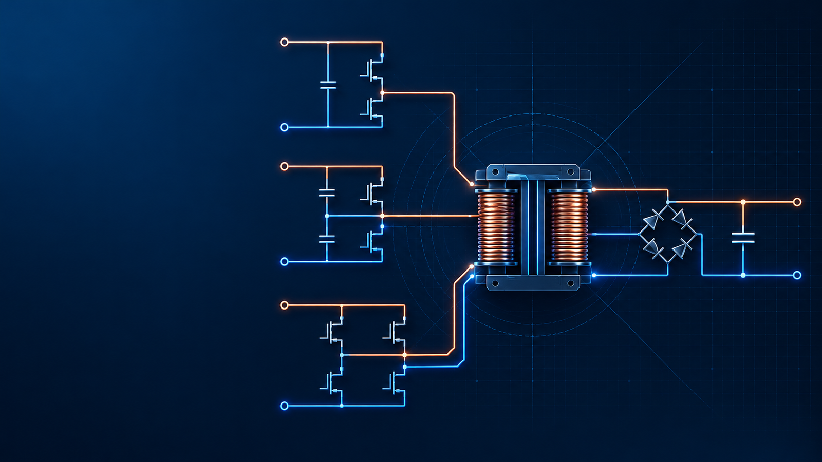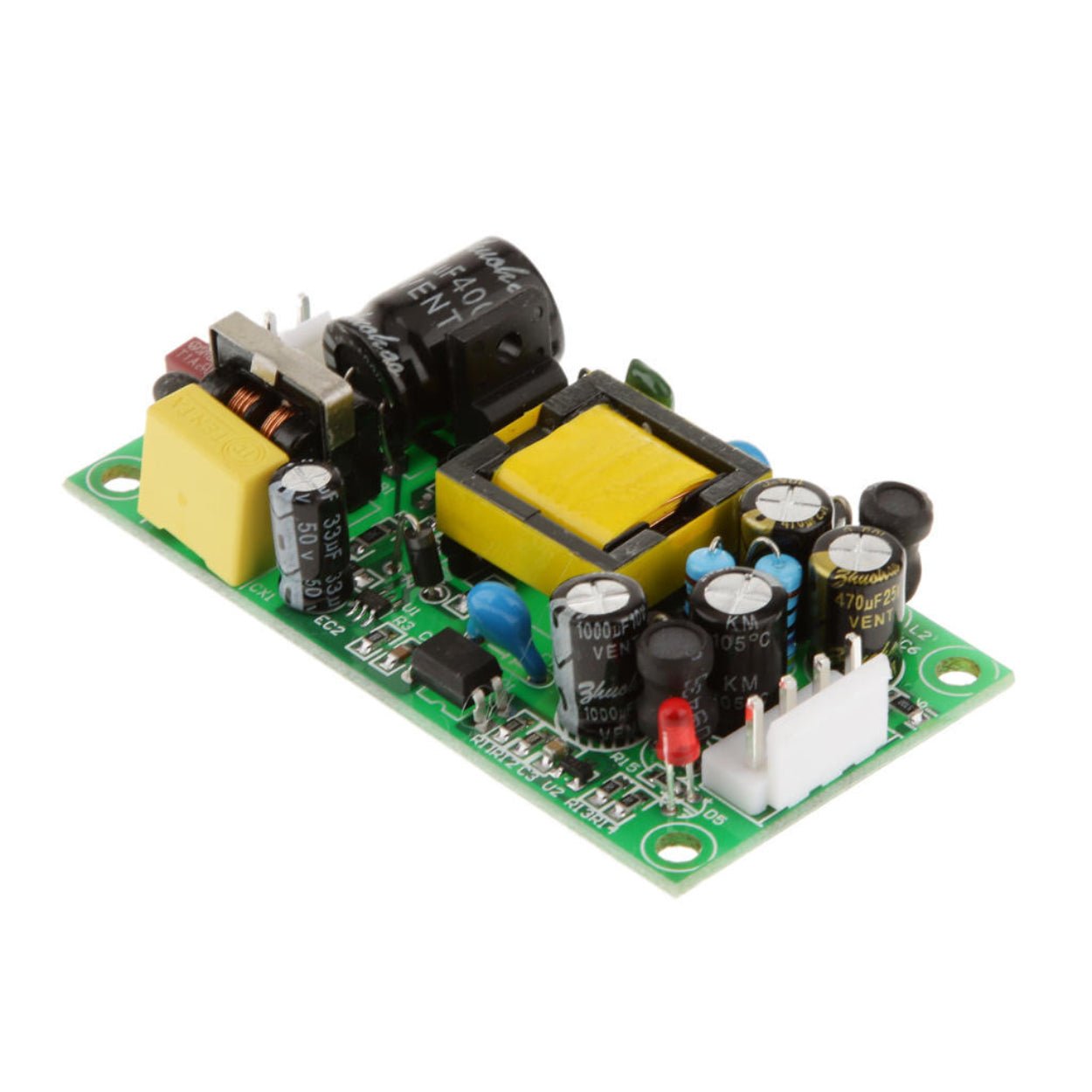
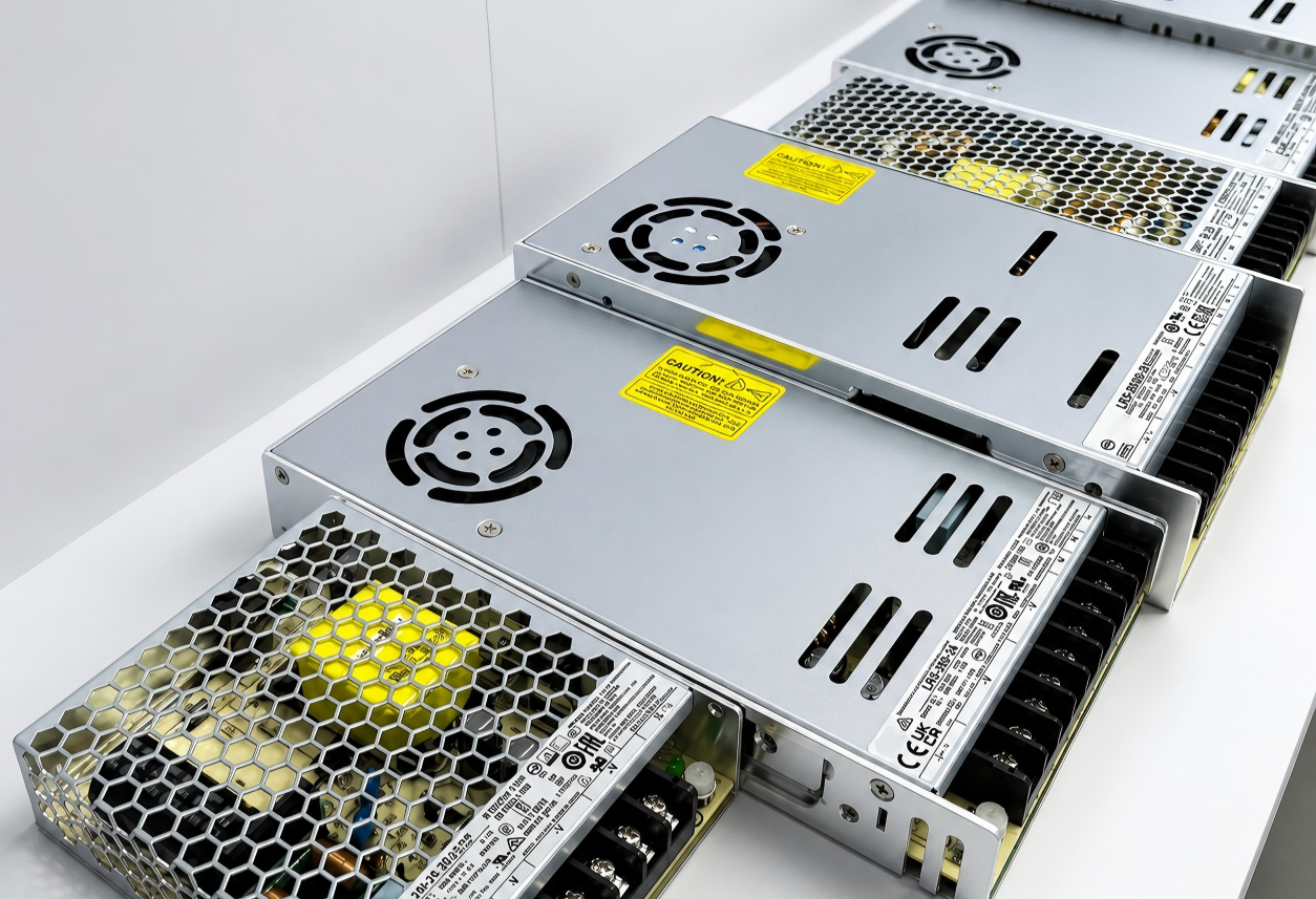
When engineers begin designing a 230V AC to 5V DC switching power supply, most of their attention is usually focused on selecting the right controller IC, calculating transformer parameters, or optimizing efficiency.
Overview
When engineers begin designing a 230V AC to 5V DC switching power supply, most of their attention is usually focused on selecting the right controller IC, calculating transformer parameters, or optimizing efficiency. These are certainly important aspects of the design process. However, many otherwise well-designed power supplies still encounter unexpected problems during testing. Some fail EMC compliance testing, some generate excessive output ripple, and others exhibit unstable behavior under dynamic loads. In many cases, the root cause is not found in the schematic at all, but in the PCB layout.
PCB design is often underestimated during power supply development. Unlike low-frequency analog circuits, a flyback power supply continuously switches hundreds of volts at frequencies ranging from tens to hundreds of kilohertz. Every switching cycle generates rapid voltage and current transitions that create electromagnetic noise throughout the system. If the layout is not carefully planned, these high-frequency energy paths can easily interfere with sensitive feedback circuits, increase conducted and radiated emissions, and ultimately reduce the reliability of the entire product.
For manufacturers developing compact chargers, industrial control systems, smart home devices, or embedded power modules, understanding how PCB layout influences performance is just as important as selecting the right components. This article examines the PCB design principles behind a typical 10W isolated flyback converter that converts 230V AC mains voltage into a regulated 5V DC output capable of supplying 2A of current.
Understanding Where Noise Actually Comes From
One of the biggest misconceptions among new power supply designers is that electromagnetic interference originates only from the controller IC or transformer. In reality, EMI is generated whenever rapidly changing current flows through a physical conductor. Every PCB trace contains parasitic inductance and resistance. When high-frequency switching currents flow through these traces, unwanted voltage spikes and electromagnetic fields are inevitably produced.
In a typical flyback converter, the primary switching loop is responsible for most of the noise generation. This loop consists of the bulk capacitor, the switching MOSFET, and the primary winding of the transformer. Every time the MOSFET turns on and off, current changes almost instantaneously, creating extremely high di/dt values. Even a small increase in loop area can significantly increase radiated emissions.
This explains why experienced power supply engineers spend considerable time optimizing current paths rather than simply focusing on component placement. A shorter current loop not only reduces EMI but also lowers switching losses and improves overall efficiency.
| Primary Switching Loop Characteristic | Impact on Performance |
|---|---|
| Small loop area | Lower EMI and improved efficiency |
| Large loop area | Increased radiated emissions |
| Long traces | Higher voltage overshoot |
| Compact routing | Better EMC performance |
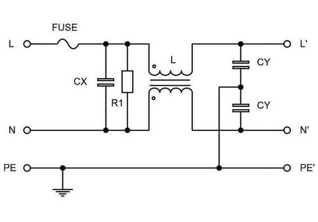
The importance of loop minimization becomes even more apparent when the design must pass CE or FCC certification. Many EMC failures can be traced directly to excessive loop areas around the switching node.
Why Isolation Is More Than a Safety Requirement
When discussing AC-DC power supplies, engineers often think about isolation primarily in terms of user safety. While electrical isolation is indeed required to protect users from dangerous mains voltages, its benefits extend far beyond regulatory compliance.
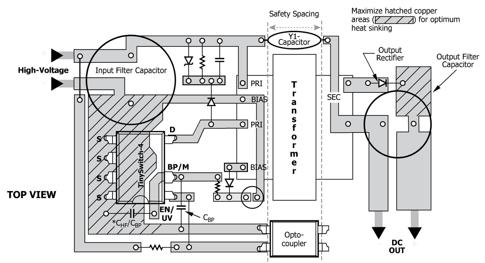
The transformer creates a physical barrier between the primary and secondary circuits, preventing direct electrical connection between the high-voltage input and low-voltage output. However, simply using an isolated transformer does not automatically guarantee adequate isolation performance. PCB layout plays a critical role in maintaining the integrity of that isolation barrier.
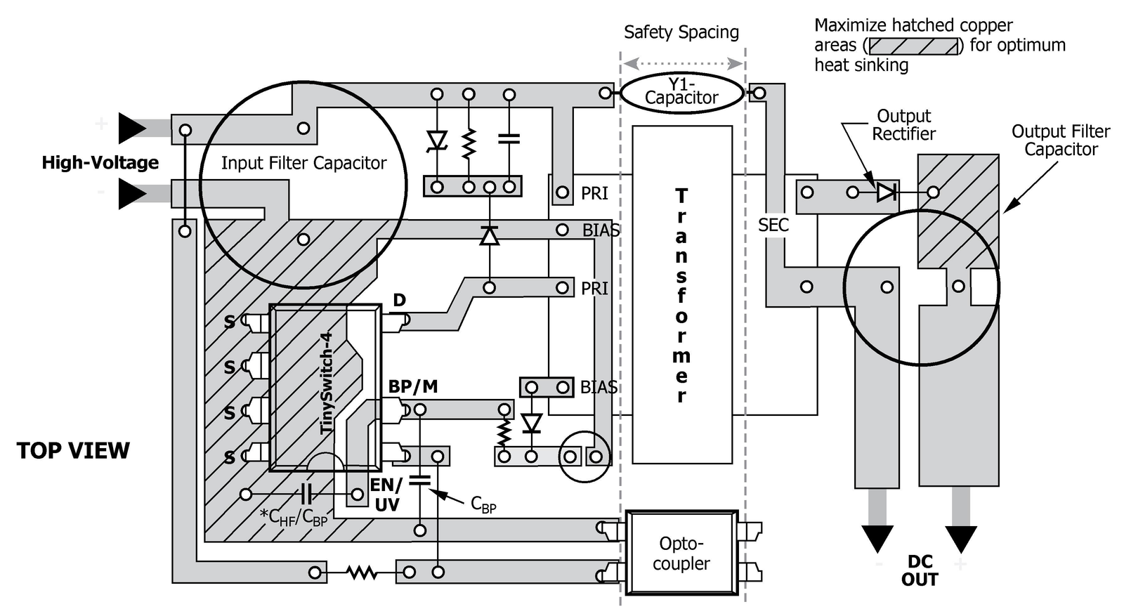
The area beneath and around the transformer deserves particular attention. Routing signal traces underneath the transformer can introduce unwanted capacitive coupling between the primary and secondary sides. This coupling provides a path for high-frequency noise to cross the isolation barrier, potentially increasing common-mode emissions and degrading output performance.
For this reason, professional power supply layouts often include isolation slots beneath the transformer. These slots increase creepage distance without increasing board size and help reduce leakage currents across the PCB surface.
| Isolation Design Method | Typical Benefit |
|---|---|
| Increased creepage distance | Improved safety margin |
| PCB isolation slots | Reduced leakage paths |
| Dedicated isolation zone | Lower common-mode noise |
| Proper transformer placement | Better EMC performance |
The result is not only improved safety compliance but also a quieter and more reliable power supply.

Why Feedback Circuit Routing Deserves Special Attention
Among all the circuits in a flyback converter, the feedback network is arguably the most sensitive. The entire regulation system depends on accurately sensing the output voltage and communicating that information back to the controller through an optocoupler.
The challenge is that the feedback signal itself is relatively small. While the primary side may be switching hundreds of volts, the feedback circuit is attempting to measure a 5V output with an accuracy of only a few percentage points. Any noise coupled into the feedback path can therefore create significant regulation errors.
Many engineers discover this problem only after measuring excessive ripple or observing unstable output voltage under varying loads. Upon closer inspection, the feedback trace is often routed too close to the transformer, the MOSFET drain node, or other noisy switching paths.
A well-designed feedback network should follow the shortest practical path between the output sensing point and the regulation components. Keeping this path away from high-current conductors reduces the likelihood of noise injection and improves regulation accuracy.
In practical designs, moving a feedback trace by only a few millimeters can sometimes achieve a greater improvement than changing multiple components.
Ground Planes Can Either Help or Hurt Performance
Ground planes are generally considered beneficial because they reduce impedance and improve current return paths. However, in switching power supplies, not all grounds are equal.
The power ground carries large switching currents generated by the MOSFET, transformer, and output rectifier. These currents contain significant high-frequency components. The analog ground, on the other hand, serves sensitive circuits such as voltage references, compensation networks, and feedback components.
If both functions share the same return path without proper planning, high-current switching noise can modulate the analog ground reference. This phenomenon, commonly known as ground bounce, can lead to inaccurate feedback measurements and unstable output regulation.
Professional PCB layouts therefore separate power ground and analog ground regions while connecting them at a carefully chosen single point. This technique allows high-current switching paths to remain isolated from sensitive control circuits while maintaining a common electrical reference.
Although ground plane design may seem like a minor layout detail, it often determines whether a power supply achieves stable operation across its entire load range.
The Relationship Between Trace Width and Reliability
Another frequently overlooked aspect of PCB design is conductor sizing. Designers sometimes focus on schematic optimization while assigning identical trace widths throughout the board. In power electronics, this approach can create significant problems.
A 5V output delivering 2A may appear modest, but even relatively low currents can generate noticeable heating when flowing through narrow traces. Excessive resistance not only causes voltage drop but also reduces efficiency and increases operating temperature.
Wider copper traces distribute current more effectively and lower resistive losses. They also improve thermal performance by spreading heat across a larger area of the PCB. For this reason, output current paths should always be noticeably wider than signal traces.
The benefits become even more important in compact enclosed products where airflow is limited and thermal margins are small.
Why Good PCB Layout Often Matters More Than Better Components
When a prototype fails EMC testing, the first instinct is often to add additional filtering components or replace major circuit elements. While these modifications can sometimes help, they rarely address the root cause.
Experienced power supply engineers understand that component quality cannot compensate for poor current paths, excessive loop areas, or improper isolation practices. A carefully designed PCB frequently outperforms a more expensive design that ignores fundamental layout principles.
This is why companies specializing in industrial power supplies invest substantial engineering resources into PCB optimization. The goal is not simply to make the circuit work, but to ensure long-term reliability, low emissions, stable regulation, and consistent performance across different operating conditions.
Conclusion
Designing a reliable 230V AC to 5V DC flyback power supply requires much more than selecting the correct controller IC or transformer. The PCB itself becomes an active part of the electrical system, influencing everything from efficiency and thermal performance to EMC compliance and output stability.
By carefully controlling switching current loops, maintaining proper isolation distances, protecting sensitive feedback circuits, separating ground references, and optimizing power trace dimensions, engineers can dramatically improve the performance of their designs. These principles are widely used throughout the power supply industry because they address the underlying physics of high-frequency power conversion rather than simply treating symptoms after problems appear.
For manufacturers seeking reliable AC-DC power solutions, PCB layout should never be considered the final step of the design process. In many cases, it is the difference between a power supply that merely functions in the laboratory and one that performs consistently in real-world applications for years to come.
Buyer Checklist
- Confirm input and output voltage before model selection.
- Check wattage, load margin and operating temperature.
- Review installation space, airflow and protection requirements.
- Share project quantity and application details for quotation support.