Radiated EMI failures in switching power supplies usually start at the source: PCB hot loops, high dv/dt copper, poor return paths, transformer parasitic coupling, and leakage-inductance ringing. This guide explains how to locate the source by frequency range, improve PCB and transformer design, and use shielding or ferrites only after the main radiator is under control.
Overview
A switching power supply can look clean on the bench and still fail radiated emissions in an EMC chamber. The output voltage is stable. Ripple is within the customer specification. Conducted emissions may even pass after a few filter changes. Then the radiated-emissions scan shows peaks between 80 MHz and 600 MHz, and the redesign conversation becomes painful.
Many teams try the visible fixes first: a larger common-mode choke, extra Y capacitance, copper tape, ferrite sleeves, shielding cans, or absorber sheets. Sometimes the peak drops by a few dB. Sometimes it moves. Sometimes the prototype passes, but a later production batch fails again because a transformer vendor changed winding tension or a PCB copper shape was slightly revised.
Radiated EMI needs a different mindset from conducted EMI. You are no longer dealing only with noise voltage on a wire. You are dealing with high-frequency energy escaping into space. In switching power supplies, that usually requires two things: a fast disturbance source and an unintended antenna. The most common places to look first are the PCB switching loops and the transformer structure.
Why radiated EMC fixes often become messy
Conducted EMI problems often respond to input filtering because the noise path is measurable at the line terminals. The design team can adjust an X capacitor, Y capacitors, differential inductance, or a common-mode choke, then check the result with a LISN and EMI receiver.
Radiated EMI is less forgiving. The emissions may come from a PCB hot loop, a switch node copper area, transformer interwinding capacitance, leakage-inductance ringing, a poor ground return, or a cable that has become an efficient radiator. Adding more filter parts at the input does not necessarily reduce a field that is being launched from the transformer window or from a long output lead.
The first step is to stop treating every failed radiated scan as a filter shortage. A filter can help when it blocks common-mode current on external cables, but it cannot repair a large high di/dt loop on the PCB. A shield can help when it is well bonded, but it can also create a new resonance if it floats or connects through a long ground path.
Analog Devices' power-supply layout guidance makes the same practical point from the PCB side: the hot loop carries the highest AC and EMI energy, and reducing its radiating effect is a primary layout task. That principle applies across many SMPS topologies, even though the exact loop changes from buck to boost to flyback.
The two sources to check first
Most power supply radiated-emissions failures are easier to understand when the design is split into two source families.
The first source is the PCB. MOSFETs, rectifiers, ceramic capacitors, transformer pins, copper pours, vias, and return paths can form loop antennas. High di/dt current produces magnetic-field radiation. High dv/dt copper produces electric-field coupling. If the loop is large or the switch node copper is generous, a small schematic error becomes a loud field problem.
The second source is the transformer. In isolated supplies, the transformer carries both magnetic energy and parasitic coupling across the isolation barrier. Leakage inductance can ring with device capacitance and PCB capacitance. Interwinding capacitance can couple primary switching noise into the secondary side, where output cables may radiate. Winding geometry, shield termination, insulation build, and air-gap orientation all matter.
Do not read frequency ranges as rigid rules, because the enclosure, cable length, topology, power level, and measurement setup can shift the peaks. As a useful debugging habit, lower radiated peaks from about 30 MHz to 200 MHz often point toward PCB loop area, grounding, and cable current. Peaks above a few hundred MHz often deserve a close look at transformer resonance, switch-node copper, diode recovery, snubber tuning, and cable coupling.
| Failed frequency range | Likely places to inspect first | Practical first checks |
|---|---|---|
| 30 MHz to 100 MHz | Power-loop area, ground-return path, input/output cable current | Near-field probe around MOSFET loop, transformer pins, bulk capacitor return, cable entry |
| 100 MHz to 200 MHz | High dv/dt copper, transformer air gap, fast rectifier loop | Reduce switch-node copper, review ground plane cuts, check snubber waveform |
| 200 MHz to 500 MHz | Transformer parasitic coupling, leakage-inductance ringing, diode recovery | Compare transformer samples, tune RC/RCD clamp, check secondary cable common-mode current |
| 500 MHz to 1 GHz | Small resonant structures, transformer winding detail, long leads, shield resonance | Shorten leads, improve shield bonding, test ferrites only after source checks |

PCB layout: the easiest place to create an antenna
PCB copper does not generate noise by itself. It decides how efficiently the converter's switching noise becomes a radiated field.
The first layout item is the high di/dt loop. In a flyback supply, the primary pulse-current path typically includes the input high-frequency capacitor, primary winding, MOSFET, and current return. On the secondary side, the rectifier diode, transformer secondary, and output capacitor form another fast-current loop. These paths should be short, tight, and visually obvious when you trace them with a pen. If the parts are scattered because the layout was optimized for convenience, the loop area increases and magnetic-field radiation rises.
The second item is the high dv/dt node. MOSFET drain copper, switching-node copper, rectifier cathode copper, and transformer pin copper can behave like small plates of an unwanted capacitor. A larger copper area can couple more electric field into nearby traces, heat sinks, transformer shields, enclosure metal, and cables. The right answer is not always the narrowest possible trace, because thermal and current needs still count. The usual design target is enough copper for current and heat, without decorative copper pour on noisy nodes.
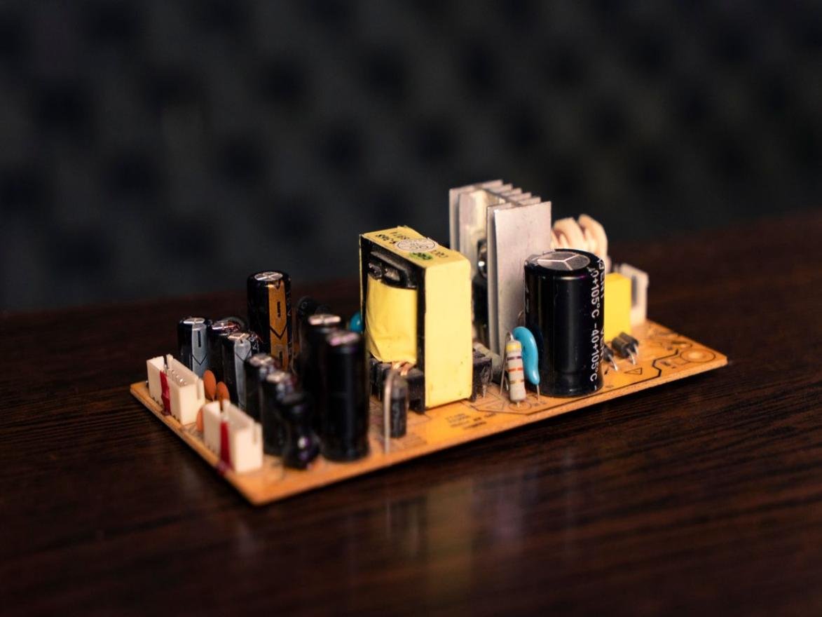
Grounding is the third item. A common mistake is to mix power ground and signal ground in a way that lets switching current share the same copper as sensing, feedback, or controller reference currents. Another mistake is to create a broken or irregular ground return, then try to fix the symptoms with capacitors. For radiated EMI, the return path is part of the antenna. Keep high-current returns compact, keep sensitive control returns quiet, and join domains at a deliberate point instead of by accident.
Cable placement completes the PCB story. Input and output leads that pass near transformer pins, MOSFET drains, rectifier loops, or snubber parts can pick up common-mode noise. Once that noise reaches a long harness, the cable can radiate more effectively than the PCB. During debug, move the cable by hand under repeatable pre-compliance conditions. If the peak changes sharply, the cable is part of the radiating structure.
| PCB issue | What it does in the chamber | Better design practice |
|---|---|---|
| Large primary or secondary pulse-current loop | Raises magnetic-field radiation, often visible below a few hundred MHz | Place MOSFET, rectifier, transformer pins, and ceramic capacitors around the smallest practical loop |
| Oversized switch-node copper | Increases electric-field coupling into nearby metal and traces | Keep high dv/dt copper compact; avoid unnecessary pours and long stubs |
| Shared noisy and quiet ground returns | Raises the emissions floor and can disturb feedback sensing | Separate pulse-current returns from control reference paths; join intentionally |
| Long unfiltered cable near noisy nodes | Turns coupled common-mode current into radiated emissions | Route cables away from switch nodes and transformer windows; add ferrites only after source reduction |
Transformer design: where high-frequency fixes often live
In an isolated switching power supply, the transformer is not just a magnetic component. It is also a high-frequency capacitive structure. Two transformer samples with the same turns ratio and inductance can behave differently above 200 MHz if the winding order, shielding, lead dress, or leakage inductance changes.
Leakage inductance is one of the usual suspects. It rings with MOSFET output capacitance, diode capacitance, winding capacitance, and PCB parasitic capacitance. If the ringing frequency falls inside the radiated-emissions measurement band, the transformer and nearby copper can radiate a narrow peak that is hard to remove with input filtering. The cure usually combines lower leakage inductance, a better winding structure, and a clamp or snubber that dissipates the ringing energy instead of letting it spray across the layout.
Interwinding capacitance is another path. Primary switching noise can cross the isolation barrier through capacitance between primary and secondary windings. Once it reaches the secondary side, the output cable may carry common-mode current. A correctly designed electrostatic shield between primary and secondary can reduce this coupling, but the shield must be terminated carefully. A shield that connects at multiple points can create a loop. A shield with a long lead may look grounded at 50 Hz and nearly floating at several hundred MHz.
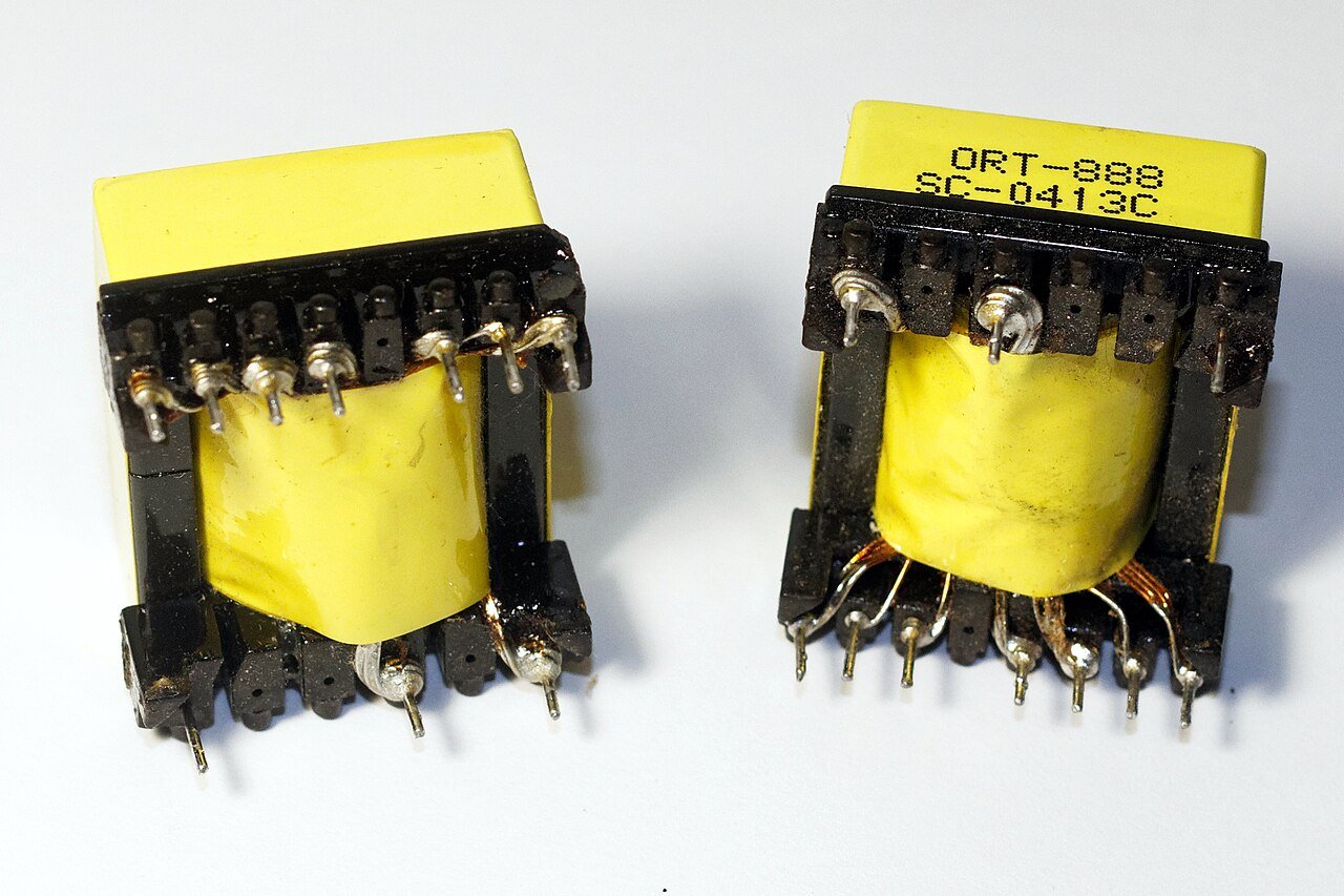
Winding consistency deserves attention during production. Loose winding, inconsistent layer build, uneven tape placement, or different start-finish lead routing can shift parasitic capacitance and leakage inductance. This is one reason a hand-built prototype can pass while a production lot is marginal. For supplier control, request leakage inductance limits, shield construction details, hipot requirements, winding drawings, and sample-to-sample comparison data.
Air-gap orientation can matter in flyback transformers. A discrete gap or poorly distributed gap can leak magnetic field into nearby copper and wiring. When the mechanical design allows it, orient the gap toward a quieter shielded region rather than toward an enclosure opening or cable path. This is not a substitute for good winding design, but it can remove a stubborn low-to-mid frequency contribution.
Snubbers, shielding, and ferrites: useful, but not first
Snubbers and clamps are important because they attack ringing energy at the source. An RCD clamp, RC snubber, diode snubber, or active clamp should be selected from measured waveforms, not copied from a similar-looking design. Watch the MOSFET drain waveform, diode waveform, temperature rise, efficiency, and EMC scan together. A snubber that removes 6 dB from a radiated peak but overheats in a sealed enclosure is not a finished fix.
Shielding can be effective when the source is already under control. A transformer shield layer, copper foil connected at one point, a bonded metal enclosure, or a local shield plate can reduce electric-field coupling. The details decide the result: short connection, low impedance, no accidental loops, stable production process, and enough clearance for safety.
Ferrites and absorber sheets are better treated as final tuning parts. They can help on cables or local hot spots, especially when the product is close to the limit. They should not be used to hide a large PCB loop or an unstable transformer design. If the bill of materials depends on several absorber patches placed by hand, production repeatability will be fragile.
A practical radiated EMI debug flow
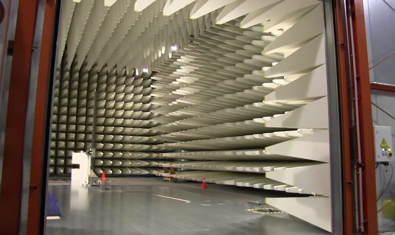
Start with the scan report. Record the failing frequencies, margin above the limit, antenna polarization, operating condition, load, input voltage, cable layout, and enclosure state. If the peak changes with cable movement, treat the cable as part of the radiation path. If it changes with a transformer swap, put the transformer build under review before changing five unrelated components.
Next, use near-field probing. Scan the MOSFET drain area, primary current loop, transformer body and pins, secondary rectifier loop, snubber, controller ground, and output cable entry. Near-field probes do not replace chamber testing, but they can show where the strongest local field sits. Keep the setup repeatable. A probe held at a different angle can tell a different story.
Then make source-level changes in a controlled order. On the PCB, shrink pulse-current loops, reduce noisy copper area, improve return paths, and separate cables from high-field regions. On the transformer, compare leakage inductance, winding construction, shield termination, and air-gap orientation. On the circuit, tune the snubber or clamp using waveform and thermal evidence.
Only after that should the team add auxiliary measures such as ferrite sleeves, absorber material, enclosure gaskets, or shield plates. Those parts are legitimate tools, but they work best after the radiator has been weakened.
| Debug step | What to do | What a useful result looks like |
|---|---|---|
| Read the chamber report | Note frequency, polarization, margin, operating mode, and cable setup | You know whether the issue is a broad floor rise, a narrow peak, or cable-sensitive radiation |
| Probe the near field | Scan hot loop, switch node, transformer, secondary loop, and cables | One or two physical regions stand out instead of the whole board looking equally noisy |
| Change one source variable | Try copper reduction, loop-area change, snubber adjustment, or transformer sample comparison | Peak moves or drops in a way that matches the suspected source |
| Confirm production control | Check PCB revision, transformer drawing, winding tolerance, and assembly routing | The fix can survive supplier and batch variation |
| Add final suppression | Use ferrites, shield bonding, absorber, or enclosure changes where needed | The product has margin without relying on hand-tuned patches |
Common mistakes to avoid
The most expensive mistake is adding a shield before understanding the radiator. A poorly bonded shield can resonate, and a floating metal part near a switch node can become a capacitive pickup plate. Shielding should have a defined RF return path.
Another mistake is increasing Y capacitance or common-mode choke size every time radiated EMI fails. Those parts mainly act on conducted common-mode current. They may reduce cable radiation, but they will not fix a hot loop radiating directly from the PCB.
Transformer shielding also gets mishandled. A primary-to-secondary shield should normally have a clear single-point termination. Multiple terminations can create a loop, while a long shield lead can lose effectiveness at high frequency. The transformer drawing should specify the shield, lead, insulation, and termination method, not leave them to workshop habit.
Finally, do not ignore copper shapes. Engineers often review trace length but miss the large copper island connected to the MOSFET drain or rectifier cathode. That copper may look harmless on the layout screen. In the chamber, it can be the difference between a pass and a long week.
What B2B buyers should ask suppliers
For OEMs, automation integrators, and industrial equipment buyers, radiated EMC is partly a supplier-control issue. Ask whether the power supply has been tested with realistic cable lengths, enclosure conditions, grounding, input voltage range, and load range. A standalone board test is useful, but it does not always represent a control cabinet, LED installation, or machine harness.
For custom or high-volume supplies, ask for evidence behind the transformer design: leakage inductance limits, shielding method, winding consistency checks, and whether alternate transformer vendors have been qualified. If the product is close to the EMC limit, small transformer changes can remove the remaining margin.
The PCB review should be just as concrete. Ask how the supplier controls hot-loop area, switch-node copper, primary-secondary spacing, ground returns, and cable routing. The best answer is not a dramatic claim about "EMC optimized design." It is a layout review, test data, and a production drawing that prevents the same problem from returning later.
Conclusion
Radiated EMI in switching power supplies is rarely solved by piling on parts at the end. The reliable path starts with the radiator: the PCB loops and copper that launch fields, and the transformer parasitics that couple and ring at high frequency.
For lower-frequency radiated problems, look hard at loop area, return paths, switch-node copper, and cable coupling. For higher-frequency peaks, compare transformer construction, leakage inductance, interwinding capacitance, shield termination, diode behavior, and snubber tuning. Filters, ferrites, absorber sheets, and metal shields still have a place, but they should finish the job, not carry the whole fix.
SIPURUI supports industrial switching power supply applications where EMC margin, layout discipline, transformer consistency, and practical production reliability all matter. If a project is facing repeated radiated-emissions failures, start the review at the PCB and transformer before approving another round of add-on suppression parts.
Buyer Checklist
- Record failing frequency, margin, polarization, input voltage, load, cable layout and enclosure state.
- Probe MOSFET loops, switch nodes, transformer pins, secondary rectifier loops and cable entry points.
- Reduce high di/dt loop area and high dv/dt copper before adding suppression parts.
- Review transformer leakage inductance, shield termination, winding consistency and air-gap orientation.
- Confirm the fix with repeatable radiated-emissions testing and production control data.