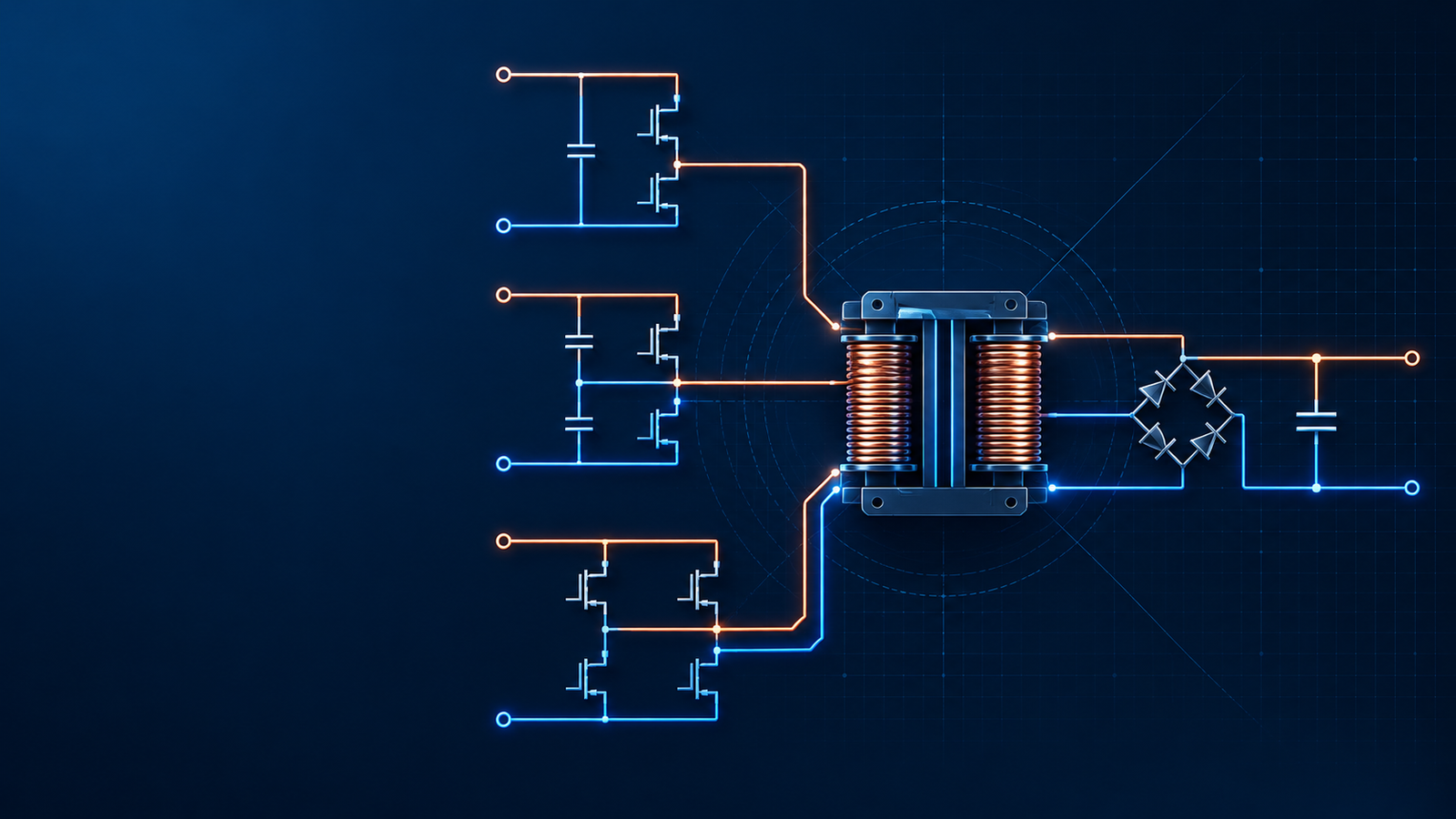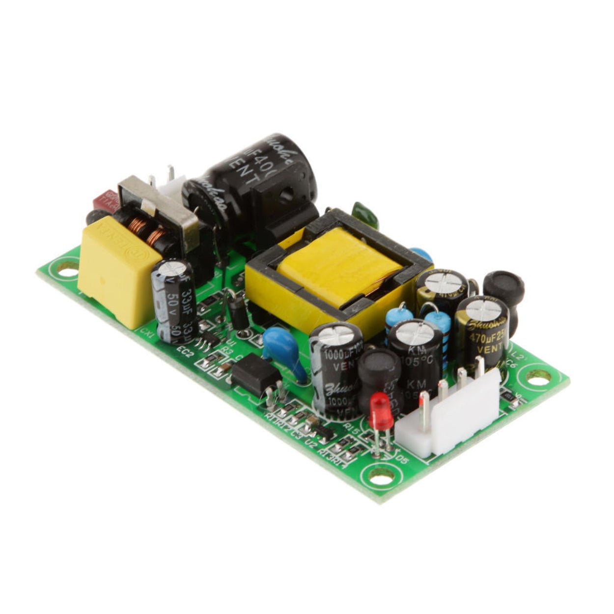
Diagnose catastrophic failure, overheating, and output oscillation in mass-produced switching power supplies with waveform-based tests and process controls.
Overview
A switching power supply can pass EVT and DVT, run for days on the engineering bench, and still fail when production reaches a few thousand units. That is not a contradiction. The prototype proves that one build can work. Mass production tests whether the design remains safe and stable across component tolerance, transformer variation, soldering quality, ambient temperature, line extremes, and operator or process variation.
The most expensive symptoms tend to fall into three groups: catastrophic failure, abnormal heating, and unstable output. They are often investigated as separate problems, but the same underlying weakness can create more than one symptom. A slow MOSFET transition may first appear as excess temperature, then become a drain overstress failure at high line. A transformer with low primary inductance can raise peak current, distort the control loop, and eventually destroy the primary switch.
This guide presents a production-oriented troubleshooting sequence. It focuses on preserving evidence, comparing failed and good units, measuring the right waveforms, and converting a one-off repair into a controlled corrective action.
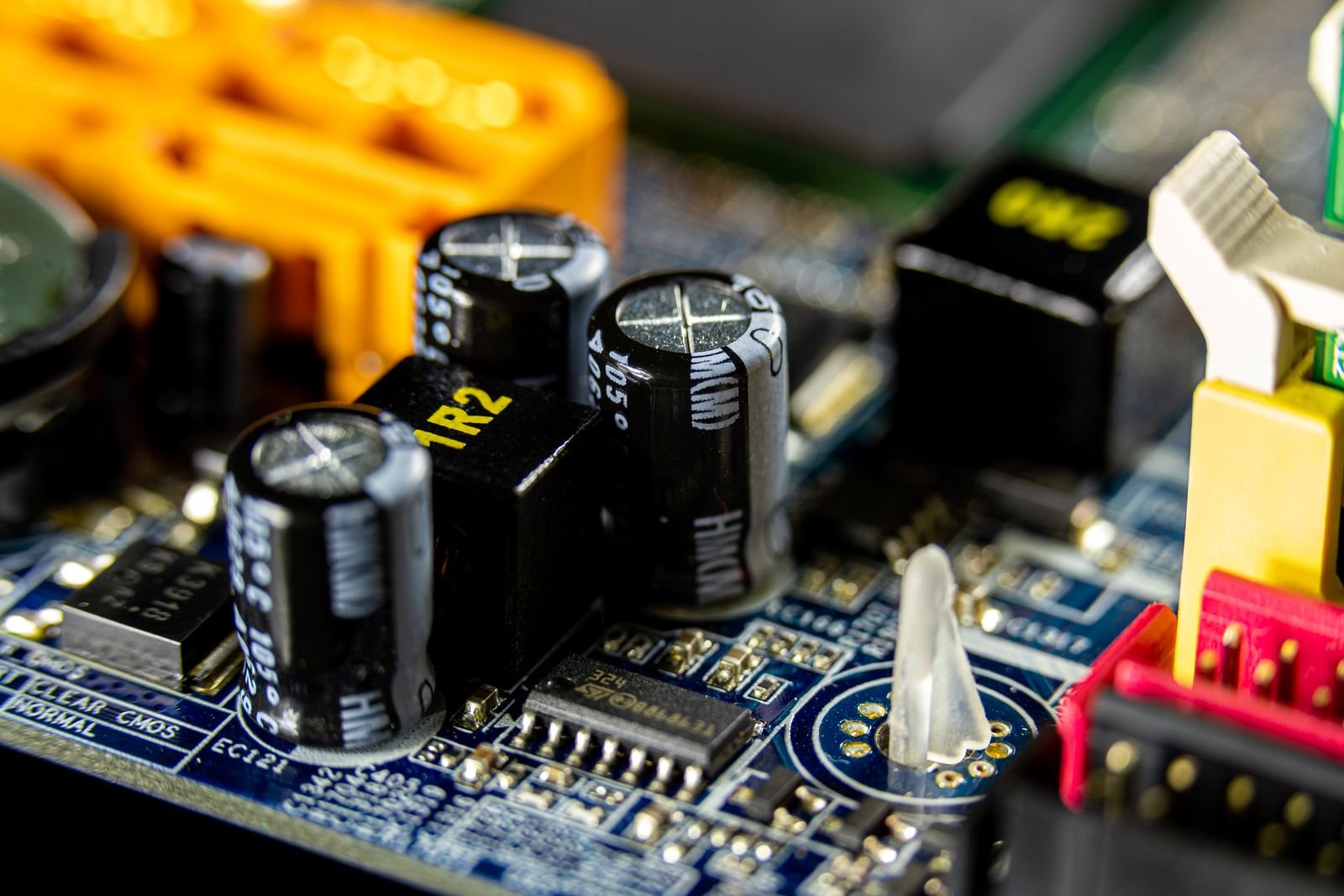
Why a proven prototype can fail on the production line
Prototype components are frequently hand-selected or purchased from a single lot. Magnetics may be wound by a sample shop, solder joints receive extra attention, and validation is often performed at room temperature with well-controlled fixtures. Production introduces a distribution rather than a single value.
The useful question is therefore not simply, "Why did this unit fail?" It is, "Which combination of electrical stress and process variation moved this unit outside the safe operating window?"
Start by separating four sources of variation:
component parameters, including MOSFET RDS(on), diode forward voltage, capacitor ESR, optocoupler CTR, and current-sense tolerance;
custom magnetics, including inductance, leakage inductance, core gap, turns ratio, winding placement, and insulation construction;
assembly, including solder voids, bridges, polarity errors, insufficient wetting, heatsink pressure, and thermal-interface coverage;
operating conditions, including input line, load profile, startup phase angle, ambient temperature, airflow, and repeated power cycling.
Do not replace the visible damaged part and immediately reapply full power. That destroys evidence and may damage a second set of parts.
First response: preserve the failure signature
Photograph the board before cleaning it. Record the unit serial number, component lot codes, transformer lot, test station, operator or line, input voltage, load, ambient temperature, and elapsed run time. Then isolate the input and discharge stored energy using the approved safety procedure for the product.
With power removed, check resistance across the input bus, primary MOSFET drain-to-source, secondary rectifier, and output rails. Inspect nearby gate resistors, current-sense resistors, clamp parts, controller supply components, and PCB traces. A shorted MOSFET is often the final event, not the first cause.
For destructive failures, use a current-limited source, isolation arrangement, differential probes, and appropriately rated current probes when the unit is energized again. Mains-referenced SMPS measurements can be lethal and can also destroy a grounded oscilloscope if the setup is wrong.

Catastrophic failure: when the supply blows a fuse or destroys silicon
"Blown power supply" is not a diagnosis. The timing and location of damage narrow the search quickly.
| Failure signature | Likely mechanisms | Measurements that separate them | Corrective direction |
|---|---|---|---|
| Fails at plug-in or power-on | Bridge or bulk-capacitor surge stress; undersized or heat-soaked NTC; MOV failure; input short; incorrect component | Startup current, rectified-bus waveform, NTC resistance versus temperature, bridge reverse-voltage rating, polarity and BOM checks | Recalculate worst-case inrush; add rating margin; revise NTC or active bypass; strengthen incoming and polarity controls |
| Primary MOSFET fails at high line | Drain overshoot from leakage inductance; inadequate clamp; excessive switching loss; transformer saturation; poor gate drive | VDS with a high-voltage differential probe, gate-source waveform, primary current ramp, clamp temperature, transformer inductance and leakage | Tune RCD/TVS/active clamp; correct winding and gap control; adjust gate drive; review MOSFET voltage and SOA margin |
| Fails only under load | Current limit too high or too slow; low transformer inductance; output overload; thermal runaway; rectifier stress | Cycle-by-cycle current, current-sense signal, load-step response, hot-unit waveforms, magnetic lot data | Set protection from worst-case tolerances; screen magnetics; add thermal derating; review semiconductor current and thermal margin |
| Secondary MOSFET or diode fails | Leakage spike; reverse recovery; synchronous rectifier timing error; ringing; inadequate voltage rating | Secondary VDS/VR waveform, gate timing, dead time, current commutation, snubber dissipation | Correct timing; add or retune snubber; improve winding coupling; select a device with justified voltage margin |
| Random units fail without a repeatable electrical corner | Solder bridge, void, cracked joint, contamination, wrong placement, damaged insulation, intermittent connector | X-ray or microsection, AOI history, ICT data, continuity while flexing or heating, lot and station correlation | Correct stencil/reflow/inspection controls; add poka-yoke; quarantine and screen the affected lot |
Measure the event, not the aftermath
Probe the primary switch drain voltage, gate voltage, current-sense node, transformer primary current, controller VCC, and output. Trigger on startup or the load transition that causes the event. A drain spike that appears safe on a 20 MHz-limited trace may be much higher when measured with a suitable probe and short loop. Conversely, a long probe ground lead can create a spike that is not present at the device. Probe technique belongs in the test method.
Review the transformer data as a distribution. Primary inductance alone is insufficient. Leakage inductance, saturation behavior, turns ratio, interwinding construction, and gap repeatability affect peak current and clamp stress. Plot results by transformer lot and compare them with failure rate.
Do not use a fixed "2x voltage rating" rule
The original design should establish semiconductor margin from measured worst-case stress, transient duration, derating policy, temperature, avalanche or surge capability, and the device safe operating area. A blanket multiplier can be wasteful in one circuit and unsafe in another. The same applies to rectifier current and inductor saturation margin.
Abnormal heating: find where the watts are going
Heat is evidence of loss. Temperature alone does not reveal whether the loss comes from conduction, switching, magnetics, or poor heat transfer.
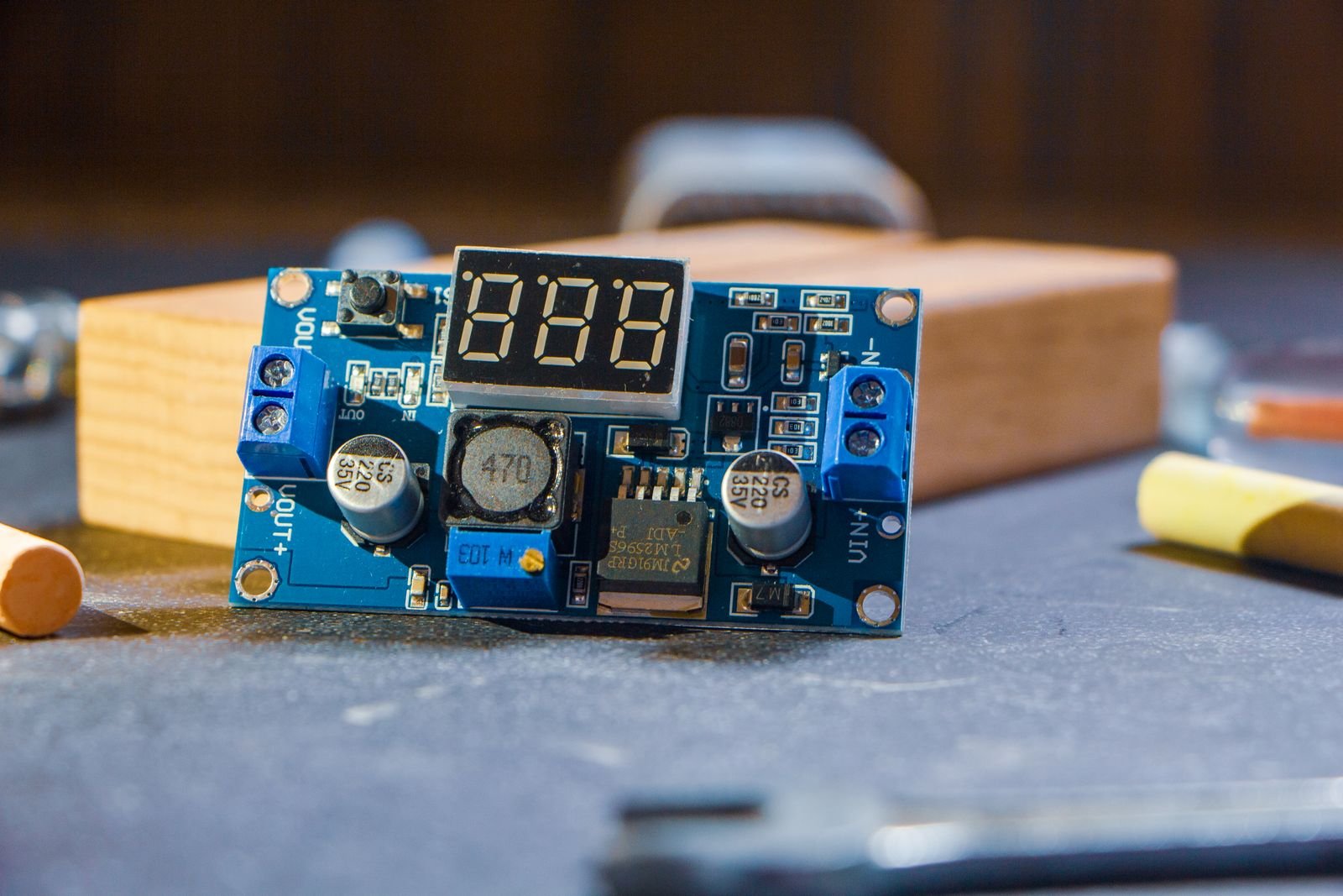
Run thermal tests at the combinations that create the largest stress: low line and full load for high RMS current, high line for switching and clamp stress, maximum specified ambient, minimum airflow, and any enclosure orientation that restricts convection. Allow the unit to reach thermal equilibrium. Use thermocouples for repeatable component readings and a thermal camera for locating unexpected hot spots; account for emissivity when reading shiny metal surfaces.
| Hot component | Common production-sensitive causes | Useful checks | Typical design or process response |
|---|---|---|---|
| Primary MOSFET | High RDS(on) at temperature; slow transitions; insufficient gate amplitude; excessive ringing; high switching frequency | VGS rise/fall and plateau, simultaneous VDS/ID, case temperature, device lot comparison | Improve driver and gate loop; rebalance gate resistance and EMI; select by hot RDS(on), gate charge, SOA, and thermal path |
| Bridge rectifier or output diode | High forward drop; RMS current above expectation; poor copper spreading; wrong package or lot | Forward drop at operating current and temperature, RMS current, solder and copper inspection | Increase thermal area; reduce conduction loss; qualify alternate lots; review package attachment |
| Transformer | Core saturation; excessive flux density; high leakage; proximity/skin loss; loose winding; core material variation | Primary current shape, no-load and load loss, inductance/leakage, winding resistance, core temperature | Tighten magnetic specification and audit; revise turns, gap, winding arrangement, or core size |
| Output inductor | Saturation current too low at temperature; high DCR; wrong core material; excessive ripple | Inductor current waveform, hot inductance, DCR, core and winding temperatures | Select using hot saturation and RMS current; reduce ripple; improve copper or core size |
| Electrolytic capacitor | Ripple current above rating; elevated ESR; proximity to hot parts; poor ventilation | Ripple current, ESR versus temperature/frequency, can temperature, capacitance and lot data | Use a suitable ripple-current/life rating; move from heat source; improve airflow and qualification |
For a MOSFET, separate conduction loss from transition loss. Conduction loss rises with current squared and with the hot value of RDS(on). Switching loss increases when voltage and current overlap during turn-on or turn-off; gate charge, driver impedance, switching frequency, parasitics, and diode recovery all matter. Analog Devices' power-supply guidance describes these mechanisms and the tradeoff between RDS(on) and gate charge.
Do not publish a universal rule such as "MOSFET temperature rise must be below 60 degrees C." Acceptable limits depend on junction rating, measured case-to-junction path, ambient specification, insulation class, capacitor life, safety approvals, and the manufacturer's derating policy. Translate measured case temperature into a credible junction-temperature estimate and retain margin at the worst production corner.
Output oscillation and jitter: classify the waveform first
An unstable output can come from the control loop, but it can also come from burst mode, current-limit interaction, controller VCC hiccup, noise injected into feedback, intermittent soldering, or an unrealistic electronic-load setting. The waveform should drive the investigation.
| Observed behavior | What it suggests | Confirmatory test | Corrective direction |
|---|---|---|---|
| Low-frequency start-stop or hiccup | Controller VCC falls through UVLO; overload protection cycles; auxiliary winding is poorly regulated | Measure VCC, gate drive, output, and current limit on the same time base | Resize VCC storage; correct auxiliary supply; review startup load and protection timing |
| Ringing after a load step | Low phase margin, output capacitor/ESR shift, current-limit interaction, or measurement/load-fixture resonance | Compare load-step response across line/load; measure loop gain where valid; change fixture and capacitor lot | Retune compensation from measured plant; control capacitor bias/ESR; improve fixture |
| High-frequency random noise | Probe pickup, switch-node coupling into feedback, poor grounding, inadequate high-frequency decoupling | Use a spring ground or coax tip; inspect FB and reference nodes; near-field probe the noise source | Reroute quiet feedback; filter at the receiving node; reduce high-di/dt loop area |
| No-load periodic ripple | Burst/skip mode, minimum-load issue, optocoupler operating point, VCC cycling | Compare with controller operating-mode specification; add controlled preload for diagnosis | Adjust preload or control strategy; correct auxiliary bias; verify no-load requirement |
| Oscillation only on some lots or at temperature | Optocoupler CTR distribution, capacitor ESR/capacitance shift, inductor variation, controller or reference tolerance | Lot-to-lot component characterization, hot/cold loop response, substitution with known-good parts | Set parameter windows; qualify lots; redesign compensation for worst-case plant variation |
Use both time-domain and frequency-domain evidence
A load transient is fast to run and shows large-signal behavior. Multiple decaying peaks after a step often point toward low damping. A loop-gain measurement provides crossover frequency, phase margin, and gain margin, but it must be injected and measured correctly. Texas Instruments notes that parasitics and component variation can materially change the measured response; it also shows the relationship between phase margin and load-step ringing.
A target near or above 45 degrees is common, but it is not a substitute for checking the actual topology, operating mode, line/load corners, temperature, and production tolerances. For isolated supplies, optocoupler CTR variation and the output capacitor's bias- and temperature-dependent behavior can move the loop significantly.
Output ripple measurement also deserves discipline. Use a short ground connection or coaxial method, define bandwidth, and keep the probe away from the switch node. Poor probing can turn common-mode pickup into a false ripple problem.
A production troubleshooting sequence that scales
The fastest path is a controlled comparison between a failed unit, a marginal unit, and a known-good unit from the same build.
Contain the lot. Stop shipment, identify the affected build window, and preserve representative failed and passing samples.
Reproduce the signature. Match line, load, temperature, startup timing, airflow, and fixture conditions. Record the exact trigger.
Localize the energy path. Determine whether the first abnormal event begins at the input, primary switch, magnetics, secondary rectifier, feedback loop, or assembly connection.
Compare waveforms and distributions. Overlay key waveforms and plot suspect parameters by supplier lot, transformer lot, and production station.
Change one variable at a time. Substitute a known-good transformer, MOSFET lot, capacitor, or controller only after baseline data is saved.
Confirm root cause at both ends. Make the failure disappear with the corrective change and, where safe, make it return by restoring the suspect condition.
Convert the fix into control. Update the specification, test limit, PFMEA, control plan, work instruction, incoming inspection, and validation matrix.
What engineering and purchasing should require before ramp
Production robustness starts in design verification, but purchasing and supplier quality own part of the result. A component approved only by headline voltage, current, or capacitance is not fully qualified for a switching supply.
| Control area | Minimum evidence before mass production | Warning sign |
|---|---|---|
| Electrical stress | Worst-case waveforms at high/low line, load extremes, startup, short circuit, hot and cold; documented derating | Rating selected from nominal values or one room-temperature sample |
| Magnetics | Controlled drawing and test limits for inductance, leakage, turns ratio, hipot, winding construction, and lot traceability | Supplier controls only inductance at one frequency |
| Thermal | Equilibrium temperatures in the final enclosure and orientation; junction or hotspot estimates; airflow tolerance | Open-bench test used as enclosure qualification |
| Loop stability | Measured load transients and loop response where applicable across component, line, load, and temperature corners | Compensation copied from a typical application without measurement |
| Manufacturing | AOI/X-ray/ICT coverage linked to known failure modes; traceability to station and material lot | End-of-line functional pass is the only control |
| Alternate parts | Side-by-side electrical, thermal, EMI, protection, and reliability evidence | Alternate accepted because the datasheet headline values match |
Closing the gap between the bench and the line
Catastrophic failure, overheating, and output oscillation are different symptoms of the same production challenge: the real build has more variation than the prototype. A robust investigation preserves the first failure signature, measures the operating event with a safe and repeatable setup, and tests the full distribution rather than the average unit.
For buyers, the practical takeaway is to ask suppliers for stress-margin data, magnetic controls, thermal results in the final enclosure, loop evidence, and lot traceability. For engineers, the goal is a design whose protection and stability remain intact when several tolerances move in the wrong direction at once.
SIPURUI can support application review, sample validation, and production-oriented power-supply selection for OEM equipment. Share the input range, load profile, enclosure, ambient, and compliance targets early; those details determine whether a supply is merely functional or ready for repeatable production.