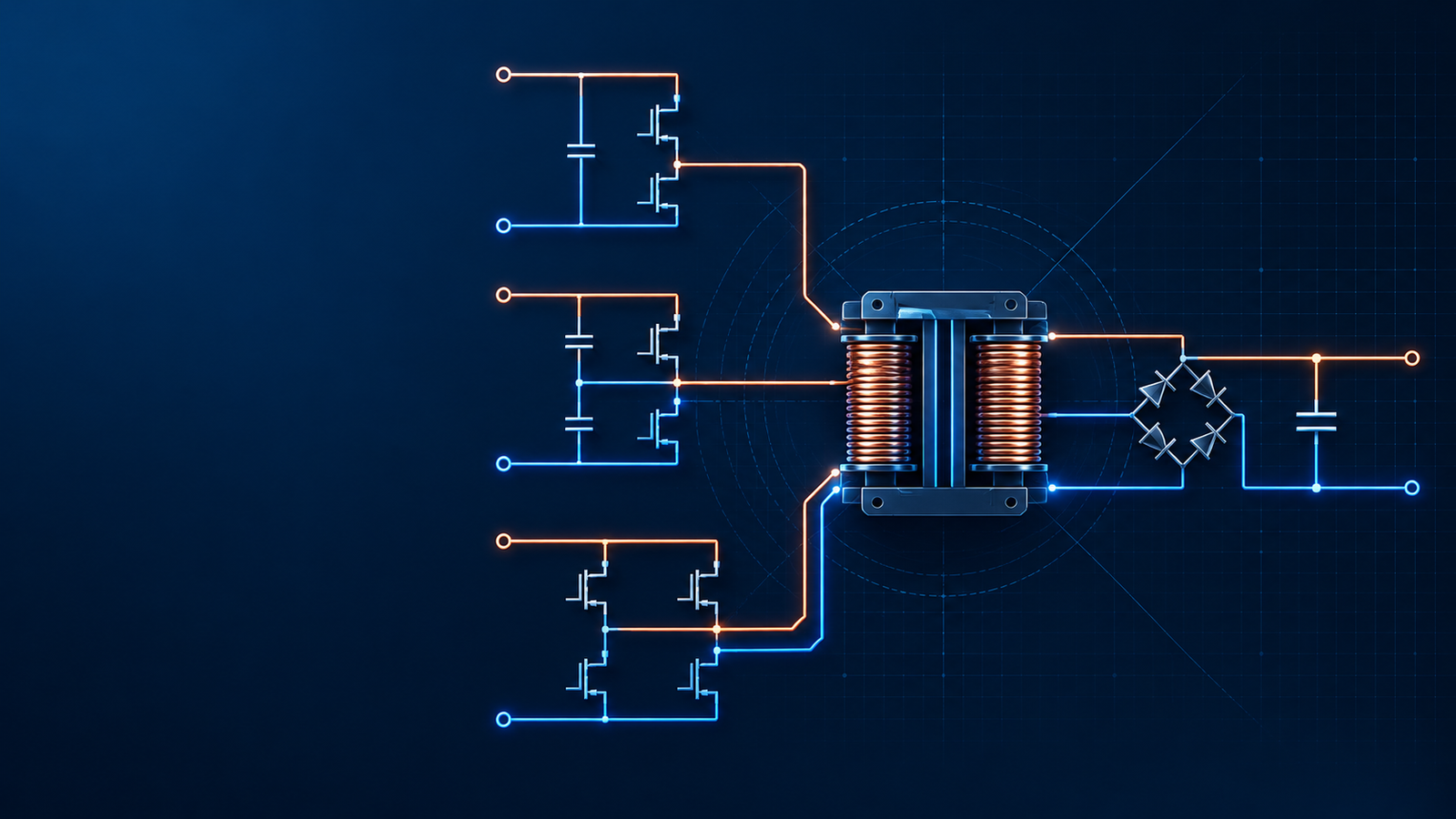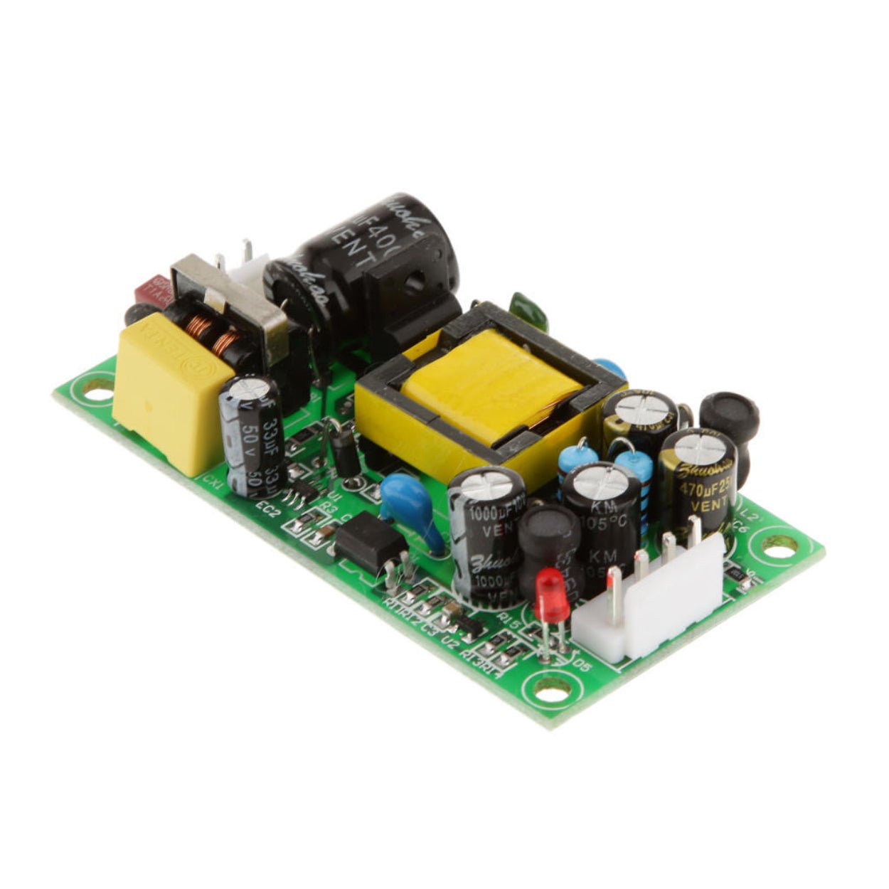
See where switching power supply efficiency is lost across MOSFETs, rectifiers, magnetics, capacitors, control circuits, filters, and interconnects.
Overview
A switching power supply may be 90% efficient, but the missing 10% does not disappear in one component. It is spread across semiconductor conduction, switching transitions, magnetic components, capacitors, control circuits, rectifiers, clamps, PCB traces, and sometimes the input EMI filter. Which term dominates changes with input voltage, output load, switching frequency, topology, and temperature.
That is why a single efficiency number is not enough for design review or supplier evaluation. A power supply can meet its nameplate efficiency at room temperature and still run a MOSFET, transformer, or electrolytic capacitor too hot for the required service life. The useful question is not simply "How efficient is it?" but "Where is the loss generated under the operating conditions that matter?"
Efficiency is simply the share of input power that reaches the load. Everything else becomes loss, usually heat. For a 240 W supply, 92% efficiency corresponds to about 20.9 W of internal loss. Raising efficiency to 95% reduces that loss to about 12.6 W. The three-point improvement removes more than 8 W of heat from the enclosure, which can change the heatsink, fan, component temperature, and lifetime calculation.
The main loss categories at a glance
The categories below apply broadly to AC-DC and DC-DC converters, although their relative importance differs by topology.
| Loss category | Main cause | Usually becomes more important when | Typical evidence |
|---|---|---|---|
| MOSFET conduction | Current through RDS(on) | Load current and junction temperature rise | MOSFET case temperature; calculated RMS current |
| MOSFET switching and drive | Voltage-current overlap, output capacitance, gate charge | Switching frequency, bus voltage, or transition time rises | VDS and ID waveforms; gate waveform |
| Rectification | Diode forward drop, recovery, or synchronous MOSFET resistance | Output current rises or output voltage falls | Rectifier temperature; dead-time waveform |
| Magnetics | Winding resistance, skin/proximity effects, core hysteresis and eddy currents | RMS current, frequency, flux swing, or temperature rises | Winding/core temperature; current waveform |
| Capacitors | Ripple current through ESR | Ripple current or ESR rises | Capacitor temperature; ripple-current measurement |
| Control and auxiliary circuits | IC bias, drivers, optocoupler/TL431 current, housekeeping rail | Output load falls | No-load and standby input power |
| Clamp, snubber, EMI, and interconnect | Leakage energy, damping, filter resistance, bridge drops, PCB resistance | Parasitics, current, or voltage spikes increase | Hot snubber parts, bridge, choke, connector, or copper area |
MOSFET losses: conduction, switching, and gate drive
The power MOSFET is often the first component engineers examine, but its loss is not a single number.
Conduction loss
When a MOSFET is on, it behaves approximately like a resistance. Its conduction loss rises with the square of RMS current and in direct proportion to RDS(on). This is why a modest increase in load current can create a much larger increase in heat. The RMS current must reflect the real switching waveform and the time for which the device conducts.
RDS(on) is temperature dependent. A device that looks comfortable at 25 degrees C can dissipate substantially more power after the junction heats up. A credible loss budget therefore uses the resistance at the expected junction temperature, not only the headline value on the first page of the datasheet.
Choosing a MOSFET with lower RDS(on) is helpful, but a larger die often carries more gate charge and output capacitance. That can reduce conduction loss while increasing dynamic loss. The best part is the one that minimizes total loss in the actual converter, not the one with the lowest isolated resistance value.
Switching transition loss
During turn-on and turn-off, drain voltage and current overlap for a finite time. In a hard-switched converter, the resulting loss generally increases with bus voltage, switched current, transition time, and switching frequency. That relationship is useful for understanding the design direction, but it is not a complete prediction. Real loss also depends on nonlinear output capacitance, diode recovery, leakage inductance, layout, driver strength, and whether the converter achieves zero-voltage or zero-current switching.
Faster edges reduce voltage-current overlap but raise dv/dt and di/dt. The result may be more ringing, common-mode noise, overshoot, and EMI trouble. Adding gate resistance slows the edge and may make compliance easier, but it also increases switching loss. Gate resistance is therefore a tuning element, not a free cure for noise.
Gate-drive and capacitance loss
The driver charges and discharges the MOSFET gate every cycle, so gate-drive loss grows with total gate charge, drive voltage, and switching frequency. MOSFET output capacitance also stores energy that may be dissipated each cycle in a hard-switched circuit. At high voltage and high frequency, these dynamic losses can materially change the device comparison. Datasheet switching energy measured under a relevant test condition is usually more useful than a calculation based on one nominal capacitance value.

Rectifier and synchronous-rectifier losses
In a diode rectifier, conduction loss is broadly set by average forward current and the diode's forward-voltage drop. This becomes painful on a low-voltage, high-current output. A 0.5 V drop represents 10% of a 5 V output voltage before other losses are counted. Schottky diodes are widely used at suitable voltage ratings because their forward drop is low and they do not exhibit the same minority-carrier reverse recovery as PN junction diodes. They still have junction-capacitance loss and reverse leakage, which can increase sharply with temperature.
Fast-recovery PN diodes add reverse-recovery current during commutation. That current heats the diode and increases turn-on stress in the opposing switch. The effect grows with switching frequency and commutation speed.
Synchronous rectification replaces the diode drop with MOSFET conduction loss. It can improve efficiency greatly at low output voltage, but only if the timing is controlled. Dead time forces current through a body diode, while insufficient dead time can turn both devices on together and cause shoot-through. The loss review should include the synchronous MOSFET RDS(on) at temperature, switching energy, body-diode interval, and driver consumption.
Magnetic losses in transformers and inductors
Magnetic components have two broad loss families: winding loss and core loss. They also create parasitic behavior that moves loss into clamps and semiconductors.
Winding or copper loss
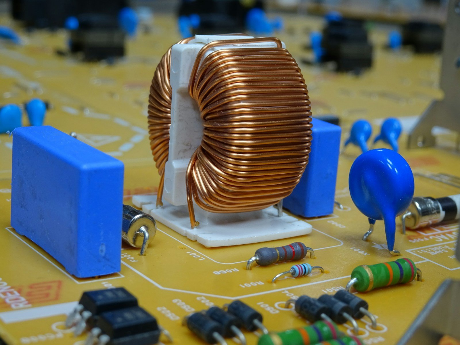
DC copper loss follows I^2R, but the winding's AC resistance rises with frequency because of skin effect and proximity effect. High ripple current can therefore produce more heat than a DC resistance measurement suggests. Simply using thicker wire does not always solve the problem; it may worsen eddy-current distribution or make the winding difficult to arrange with low leakage.
Foil, parallel strands, and litz wire are options, but each belongs to a particular frequency, current, fill-factor, insulation, and cost range. The winding arrangement also affects capacitance, leakage inductance, and manufacturability. A transformer that is efficient in the first prototype can drift in production if winding placement is not controlled.
Core loss
Core loss comes mainly from hysteresis and eddy-current mechanisms. It is sensitive to material, frequency, peak flux density, flux swing, waveform shape, temperature, air gap, and manufacturing condition. The common statement "higher frequency means more core loss" is directionally correct, but incomplete: designers may reduce flux swing or change core size and material when frequency changes.
Use the core manufacturer's data or an appropriate Steinmetz-based model with the real waveform. A sine-wave chart applied directly to a high-duty rectangular waveform can give a false result.
Leakage-inductance loss
In a flyback converter, leakage energy appears as a drain-voltage spike when the primary switch turns off. A dissipative RCD or RC clamp converts much of that energy into heat. Reducing leakage inductance through winding design can lower clamp loss, but it may increase interwinding capacitance and common-mode noise. Active-clamp and energy-recovery approaches can reclaim part of the energy, at the cost of extra circuitry and control complexity.
Capacitor ESR and ripple-current loss
Capacitors are not lossless storage elements. Ripple current flowing through equivalent series resistance produces heat, and that heat rises with the square of RMS ripple current. A capacitor that sees twice the ripple current can therefore experience roughly four times the ESR-related loss if its ESR remains unchanged.
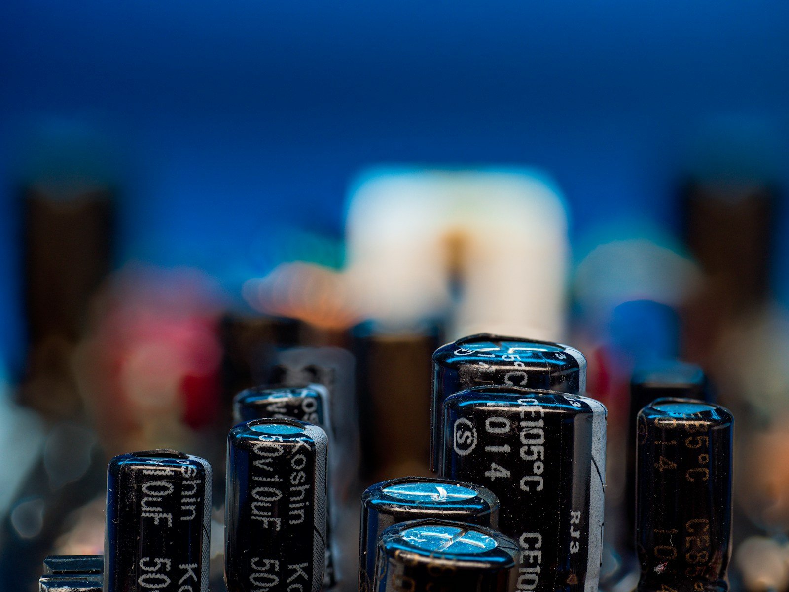
The RMS ripple current is different at the input and output and changes with topology and operating point. Aluminum electrolytic capacitors must be checked against ripple-current rating at the relevant frequency and ambient temperature. Their ESR also changes with temperature and age. Ceramic capacitors have very low ESR, but DC bias can reduce effective capacitance, and high ripple current can still create dielectric loss.
Temperature is the reliability bridge between electrical loss and field life. A capacitor that remains within its voltage rating can still age quickly if ripple heating places its hot spot near a transformer, rectifier, or heatsink.
Control, auxiliary, standby, and light-load losses
The PWM controller, isolated feedback circuit, gate drivers, current-sense network, auxiliary winding, relays, fans, and housekeeping supply all consume power. At full load, these watts may be a small percentage. At no load or light load, they can dominate.
Optocoupler LED current and TL431 bias are common examples in isolated supplies. Startup resistors can also waste continuous power unless they are disconnected after startup. Many controllers improve light-load efficiency through pulse skipping, burst mode, variable frequency, or device shutdown. These modes reduce the number of switching events but may create audible noise, larger output ripple, or a different EMI signature.
This explains why a supply can show good peak efficiency and disappointing efficiency at 5% load. For industrial systems that spend most of their life in standby or partial load, the efficiency curve matters more than the single best number.
Losses in bridges, clamps, EMI filters, PCB copper, and connections
The input bridge conducts through two diode drops on each half-cycle. At higher power, the bridge can be a visible thermal hot spot. Totem-pole PFC or synchronous input rectification can reduce this loss, but the control and EMI design become more demanding.
Snubbers and clamps trade voltage stress and ringing for deliberate dissipation. If an RCD clamp runs hot, check transformer leakage, clamp voltage, switching timing, and the actual energy per cycle before increasing resistor wattage.
Common-mode and differential-mode chokes add copper and core loss. NTC inrush limiters remain resistive after startup unless bypassed. Current-sense resistors, connectors, relay contacts, PCB traces, and vias also matter in high-current paths. None may dominate alone, but together they can consume the margin left after semiconductor and magnetic optimization.
How operating conditions change the dominant loss
| Operating condition | Losses that tend to grow | Design implication |
|---|---|---|
| High load current | MOSFET conduction, winding copper, rectifier, PCB and connector loss | Check hot RDS(on), RMS current, copper cross-section, and airflow |
| High input voltage | Switching overlap, Coss energy, clamp stress, some core-loss conditions | Review switching energy, overshoot, and high-line efficiency |
| High switching frequency | Switching, gate drive, magnetic AC, core, and capacitive loss | Smaller magnetics are bought with a tighter thermal and EMI budget |
| Low output voltage and high current | Rectifier drop or synchronous MOSFET conduction | Synchronous rectification often has the strongest payoff |
| Light or no load | Controller bias, auxiliary rail, gate drive, repeated switching events | Use an appropriate light-load mode and measure standby power |
| High ambient temperature | RDS(on), diode leakage, capacitor aging, cooling limitation | Derate output or improve thermal path; verify at worst-case ambient |
The real design tradeoffs
Higher switching frequency can shrink the transformer, inductor, and sometimes the filter capacitors. It also increases the number of switching transitions and usually raises gate-drive, core, and AC winding loss. The correct frequency is an economic and thermal decision, not a contest for the smallest magnetic component.
The MOSFET tradeoff is similar. Very low RDS(on) may arrive with higher Qg and Coss. A slower gate edge may reduce overshoot and EMI but consume more power during the transition. Lower transformer leakage can reduce clamp loss yet raise primary-to-secondary capacitance. Every improvement should be checked against the losses and constraints it moves elsewhere.
Soft-switching topologies can reduce transition loss, especially at higher frequency, but they do not erase conduction, circulating-current, magnetic, drive, or control loss. Their benefit depends on whether soft switching is maintained across the required line and load range.
A practical loss-budget workflow
Do not start with a thermal camera and guess from the hottest part. Build an electrical budget first, then use temperature measurements to challenge it.
Define operating points. Include low and high line, nominal line, 10%, 50%, and 100% load, worst-case ambient, and any overload or standby requirement.
Measure input and output power correctly. Use calibrated power-analysis methods. For AC input, include power factor and harmonic current; a handheld meter is rarely enough.
Allocate the total loss. Calculate semiconductor conduction and switching loss, magnetic copper and core loss, rectifier loss, capacitor ESR loss, and fixed auxiliary consumption.
Measure waveforms at the component. Probe VDS, gate voltage, current, rectifier commutation, and ripple current with bandwidth, grounding, and deskew appropriate to the edge speed.
Map temperature after stabilization. Record ambient, airflow, enclosure state, warm-up time, emissivity assumptions, and the location of each measured hot spot.
Reconcile the budget. If the sum of calculated losses does not approach measured input-minus-output power, revisit RMS current, parasitics, temperature-dependent parameters, and uncounted auxiliary loads.
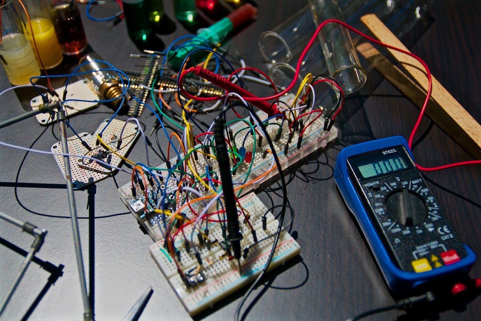
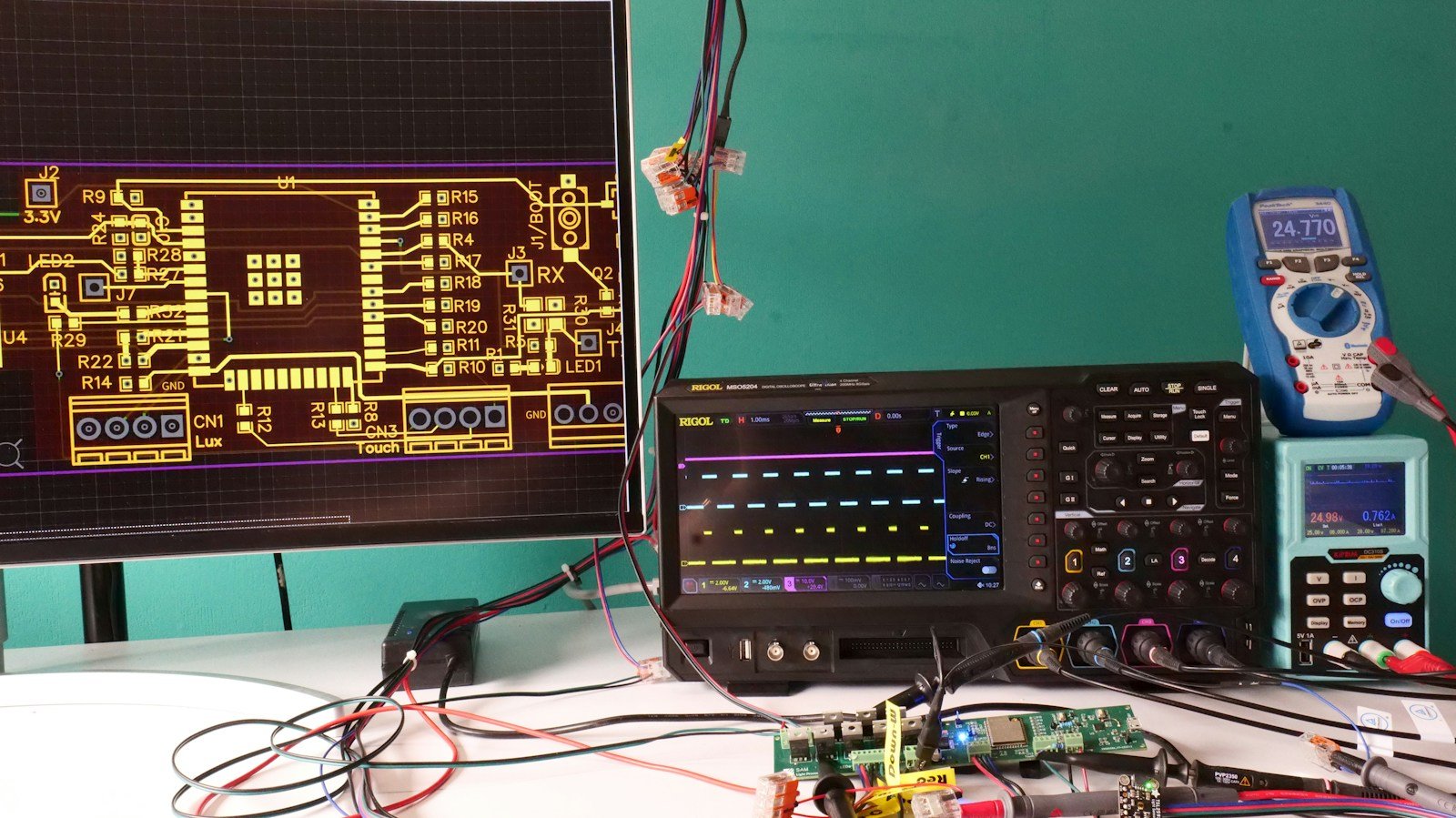
Bench data should be tied to a defined operating point; otherwise, loss comparisons are hard to reproduce. Photo: Nicolas Thomas on Unsplash, Unsplash License.
What B2B buyers should request from a supplier
| Evidence to request | What it reveals | Weak answer to watch for |
|---|---|---|
| Efficiency curve at multiple line voltages | Full-load and partial-load behavior | One peak-efficiency value with no test condition |
| Temperature-rise report at rated load | Hot components and thermal margin | Open-bench result when the product will run in an enclosure |
| Derating curve versus ambient temperature | Real usable power in the application | "Rated power" without an ambient or airflow statement |
| Standby or no-load input power | Fixed control and auxiliary loss | No distinction between enabled, disabled, and standby modes |
| Waveforms for switch stress and rectifier timing | Overshoot, ringing, recovery, and shoot-through risk | Only steady DC readings |
| BOM and magnetic construction controls | Production repeatability of the loss budget | Uncontrolled substitutions for MOSFETs, cores, wire, or capacitors |
For custom industrial supplies, the same review should cover input tolerance, overload profile, cooling orientation, altitude, enclosure temperature, expected load cycle, and any compliance-driven EMI filter changes. A late filter or snubber change can move both efficiency and temperature.
Conclusion
Switching power supply loss is a system result. MOSFETs, rectifiers, transformers, inductors, capacitors, control circuits, clamps, filters, and interconnects all contribute, and the leading contributor changes with operating point. A useful design review combines a component-level loss budget with efficiency curves, switching waveforms, and stabilized thermal measurements.
When evaluating an off-the-shelf or custom supply, ask for evidence across the actual line, load, ambient, and cooling range. SIPURUI can support that discussion with application requirements, efficiency data, derating information, and thermal validation for industrial switching power supply projects.