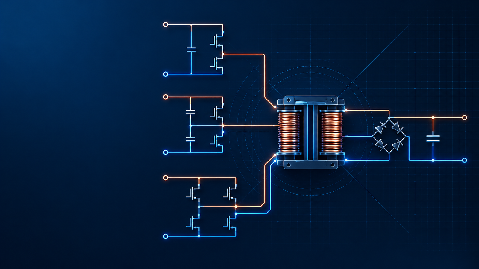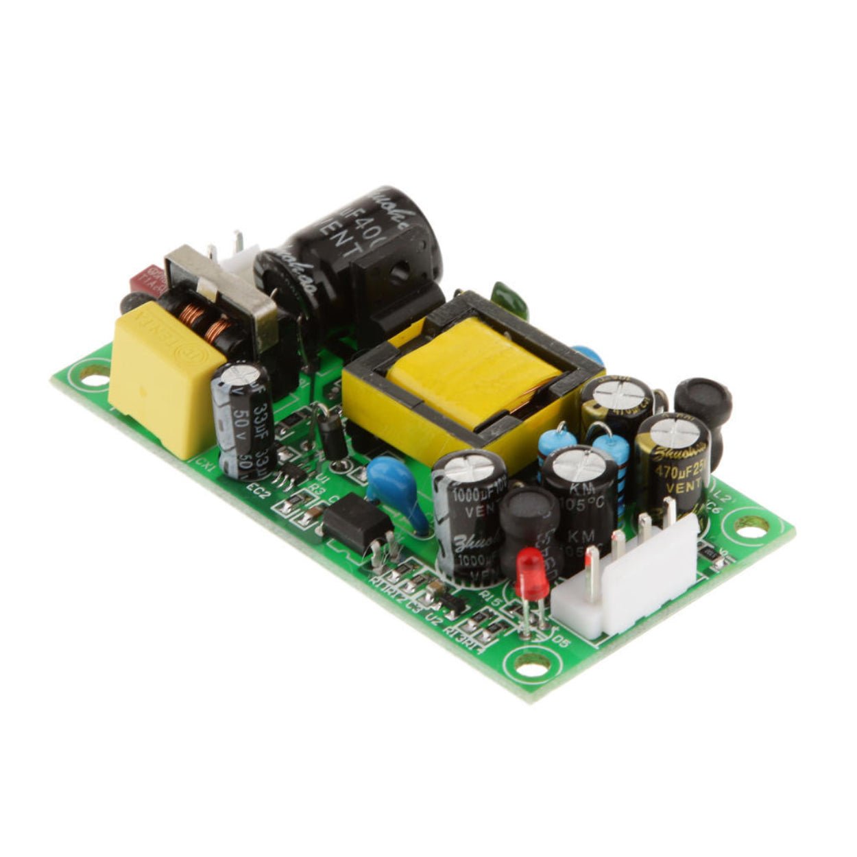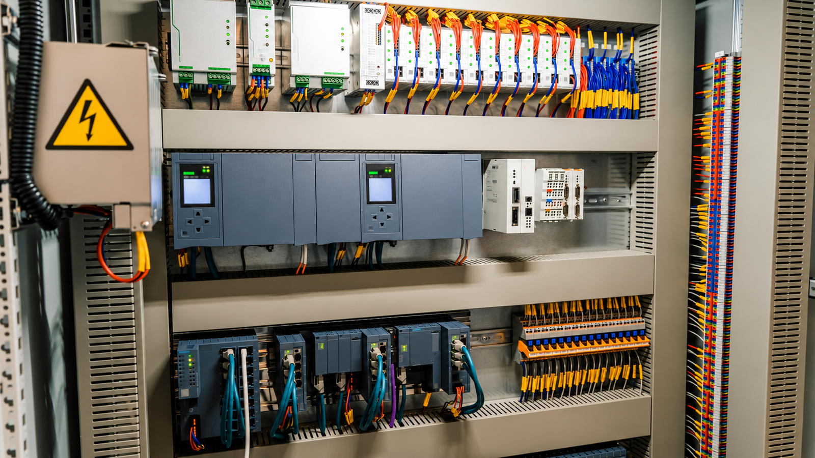
Common-mode noise is one of the reasons a switching power supply can look clean on the schematic and still fail EMC testing. This guide explains where common-mode current is generated, how it couples through parasitic paths, and which EMC fixes usually work.
Overview
Common-mode noise is one of the reasons a switching power supply can look clean on the schematic and still fail EMC testing. The input filter is present. The transformer meets the insulation requirement. The output voltage is stable. Then the conducted-emissions scan shows a stubborn high-frequency peak, or the radiated-emissions chamber turns a cable into an antenna.
That is the frustrating part of common-mode EMI. It rarely follows the neat current path drawn in the power-stage diagram. It moves through parasitic capacitance, heat sinks, transformer interwinding capacitance, PCB copper, chassis metal, protective earth, and long cables. Adding a larger common-mode choke or a bigger Y capacitor may help, but it can also move the problem, increase leakage current, or create a new resonance.
For engineers, equipment builders, and industrial power supply buyers, the practical question is not simply "Which filter should we add?" The better question is: where is the common-mode current being generated, where is it coupling, and where can it return without using the external cable as part of the noise path?
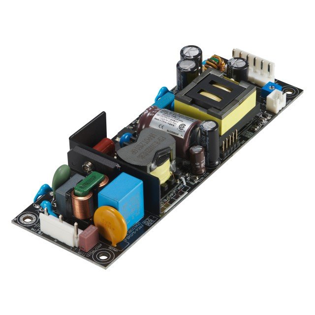
Differential-mode and common-mode noise are different problems
The first step in an EMC debug job is to avoid treating every emission peak the same way. Differential-mode noise and common-mode noise can appear in the same scan, but they have different current paths and different fixes.
Differential-mode noise flows out on one conductor and returns on the other. In an AC input supply, that means line and neutral carry opposite noise currents. It is usually tied closely to input ripple current, rectifier current pulses, and switching-frequency harmonics. Its loop is more visible, and an X capacitor, differential inductor, or input pi filter often gives a predictable improvement.
Common-mode noise is different. Line and neutral carry noise in the same direction, and the return path is somewhere else: earth, chassis, a test receiver ground, a metal enclosure, a heat sink, a control cable shield, or stray capacitance to the surroundings. Because the loop is partly hidden, common-mode noise often dominates the higher-frequency region and radiated behavior.
| Comparison point | Differential-mode noise | Common-mode noise |
|---|---|---|
| Main current path | Line to load and back through neutral, or positive rail to load and back through return | Line and neutral, or output pair, moving in the same direction with return through earth, chassis, cable shield, or parasitic capacitance |
| Typical frequency concern | Often strongest from the switching frequency up through lower conducted-emissions bands | Often troublesome at higher conducted-emissions frequencies and in radiated-emissions testing |
| Main physical driver | Pulsed input current, rectifier current, inductor ripple, loop inductance | High dv/dt nodes coupling through parasitic capacitance |
| Usual first-line components | X capacitor, differential inductor, input bulk and ceramic capacitors | Common-mode choke, Y capacitors, shields, chassis bonding |
| Debug difficulty | Easier to map because the loop is part of the power circuit | Harder because the return path may use metalwork, layout, cables, or test fixtures |
In real products the two modes interact. A poorly damped differential filter can create a peak that looks like a common-mode issue. A badly routed Y capacitor can inject high-frequency current into the wrong copper area. Still, separating the two modes early keeps the debug process from becoming trial and error.
The core mechanism: high dv/dt plus parasitic capacitance
Common-mode noise in a switching power supply is mainly a displacement-current problem. When a high-voltage node changes quickly, any nearby conductor becomes part of a small capacitor. That capacitance may be only a few picofarads, but at tens of megahertz it can carry enough current to fail a limit line.
The simplified relationship is:
`i = C x dv/dt`
That small equation explains why common-mode EMI is so sensitive to layout, transformer structure, heat-sink mounting, device speed, and cable routing. If the capacitance is larger, the coupled current increases. If the voltage transition is faster, the coupled current also increases. A fast, high-voltage drain node placed under a large copper area near the chassis is almost inviting the noise to leave the converter.
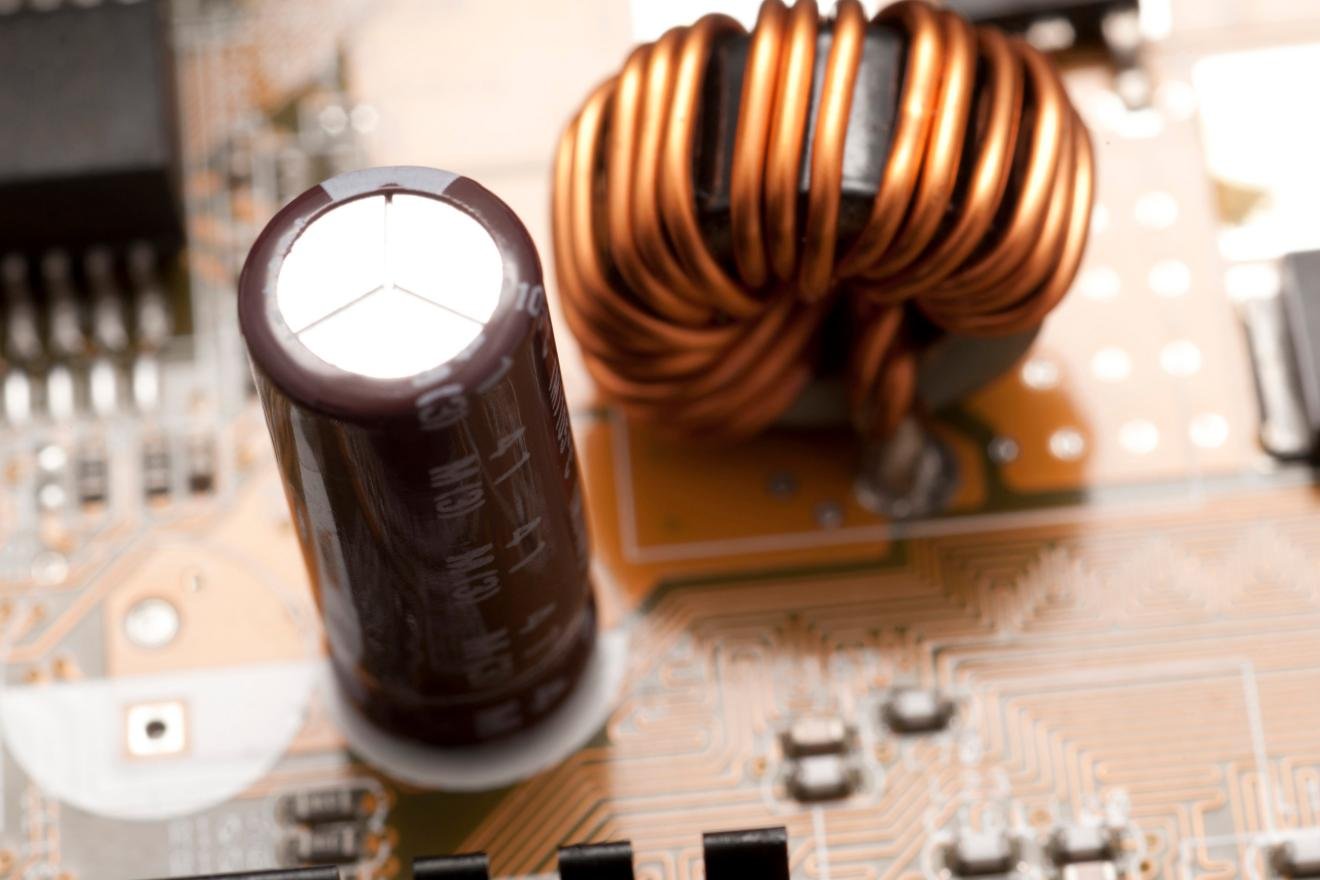

Four major sources of common-mode noise in SMPS designs
Most switching power supply common-mode problems come from a few physical locations. The exact topology matters, but the same pattern appears in flyback, forward, LLC, PFC, and DC-DC stages.
1. MOSFET drain or switch-node voltage transitions
The MOSFET drain in an offline flyback converter, the half-bridge midpoint in an LLC converter, the boost switch node in a PFC stage, and the switching node in a buck converter all have one thing in common: high dv/dt. These nodes may swing from near zero to hundreds of volts in a very short time.
If that node has large copper, long routing, tight spacing to a heat sink, or a broad overlap with another layer, it capacitively drives nearby metal. The coupled current then looks for a return path. In a Class I product it may flow through protective earth. In a Class II product it may use the output cable, enclosure capacitance, or test table coupling. Either way, the external wiring can become part of the EMI structure.
This is why a power supply can pass electrically but fail emissions after it is installed in a metal machine cabinet. The cabinet changes the parasitic capacitance and gives common-mode current a new return route.
2. Transformer interwinding capacitance
In an isolated power supply, the transformer is both the isolation barrier and a common-mode coupling path. The primary winding sees high-frequency switching voltage. The secondary winding connects to output cables, control boards, sensors, PLC modules, or field devices. The capacitance between windings lets high-frequency current cross the isolation barrier without a direct conductive connection.
This is especially important in flyback converters, where the primary drain waveform has high amplitude and sharp edges. A transformer with large winding overlap or no shield can couple noise from primary to secondary. The result is often a clean-looking DC output with high-frequency common-mode voltage riding on both output leads.
A well-designed shield winding or copper foil shield, connected at a single suitable point, can reduce this coupling. The connection point matters. A shield tied carelessly into a noisy ground node may collect noise and redistribute it. Multiple shield connections can create a loop and make the problem worse.
3. Diode reverse recovery and secondary switching spikes
Rectifier diodes and synchronous rectifier MOSFETs can be quiet at the DC level and noisy at the transition edge. A diode with hard reverse recovery creates a narrow current spike when it stops conducting. That spike excites leakage inductance, package inductance, and PCB parasitics. The frequency content can extend far beyond the basic switching frequency.
On the secondary side, these spikes may couple into output ground and output cables. On the primary side, clamp circuits and snubbers that are physically too large can create additional high-frequency loops. A faster diode is not always a quieter diode; recovery softness, junction capacitance, layout, and operating current all matter.
4. PCB layout that amplifies parasitic coupling
Layout does not create the switching event, but it decides how much of that event escapes. Large switch-node copper increases capacitance. A long drain trace increases inductance and ringing. Poorly separated primary and secondary areas increase coupling. A Y capacitor placed far from the input connector may force common-mode current across the PCB before it reaches the intended return point.
The underside of a power supply board is often more revealing than the component side. Creepage slots, ground spacing, copper pours, input-to-output separation, and chassis-bond locations all affect the actual EMI path.
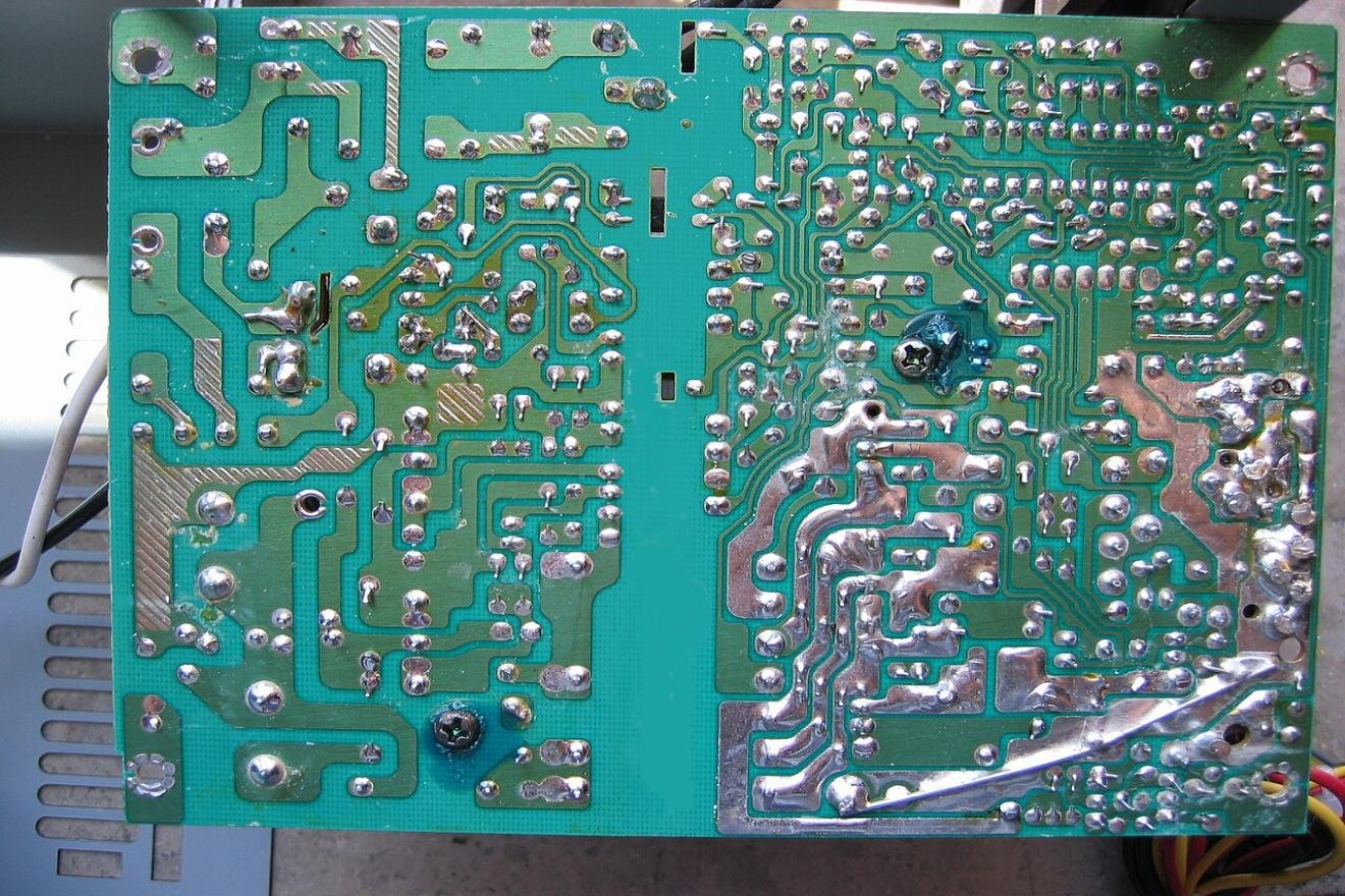
How common-mode noise travels out of the power supply
A useful way to think about common-mode noise is to follow three stages.
First, the converter creates a high-frequency disturbance at a high dv/dt node. The main switch, transformer winding, clamp node, or rectifier transition is the source.
Second, the disturbance couples through parasitic paths. That may be MOSFET drain-to-heat-sink capacitance, transformer interwinding capacitance, primary-to-secondary PCB capacitance, Y capacitor current, or capacitance from internal metalwork to the enclosure.
Third, the current leaves through an external conductor. The AC input cable, PE wire, DC output lead, control cable, sensor harness, motor cable, or machine frame may provide the physical structure that turns conducted noise into radiated emissions.
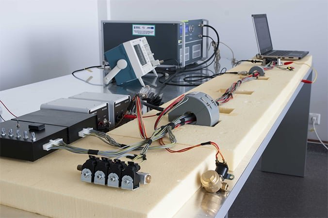
This explains why an open-frame power supply tested alone may behave differently after it is mounted in equipment. The final product changes the cable length, grounding, enclosure coupling, output loading, and mechanical spacing. EMC margin must be designed for the installed system, not just the bench prototype.
Suppression strategy: source first, path second, filter last
Common-mode filtering is important, but it should not be the only answer. A robust fix usually follows this order: reduce the noise source, control the coupling path, then use the input or output filter to finish the job.
| Fix area | Where it works best | Practical benefit | Watch point |
|---|---|---|---|
| Gate resistance and switching-speed tuning | MOSFET drain, half-bridge midpoint, PFC switch node | Reduces dv/dt and ringing at the source | Too much resistance increases switching loss and heat |
| RC/RCD snubber or clamp optimization | MOSFET drain, diode node, transformer leakage spike | Damps high-frequency spikes before they excite the structure | Parts must be placed close to the noisy loop |
| Transformer shield or winding redesign | Isolated AC-DC and DC-DC converters | Reduces primary-to-secondary common-mode coupling | Shield should use a controlled single-point connection |
| PCB copper and grounding changes | High dv/dt copper, primary-secondary boundary, chassis bond | Often gives large improvement without adding BOM cost | Requires discipline early in layout, harder after tooling release |
| Common-mode choke and Y capacitors | Input/output port filtering | Attenuates noise before it reaches external cables | Must meet leakage current, safety, voltage, and impedance requirements |
Practical fixes that usually move the needle
Start at the switching node. Keep high dv/dt copper compact. Avoid decorative copper pours tied to noisy switch nodes. Place snubbers, clamp diodes, and high-frequency capacitors tight to the devices they protect. If a heat sink is near the switch node, decide deliberately whether it should be bonded to chassis, connected through a defined impedance, or physically moved.
Then look at the transformer. For isolated supplies, the transformer is often the most important common-mode bridge. Use winding structures that reduce overlap between noisy primary sections and quiet secondary sections. Where the design allows it, add an electrostatic shield between primary and secondary and connect it to the correct quiet reference or primary bulk return point. Do not treat the shield as a random ground tab.
On the secondary side, control rectifier recovery and loop area. Choose rectifiers with suitable recovery behavior, use synchronous rectification timing carefully, and put damping parts where the spike current actually flows. Output cables are usually long enough to radiate, so secondary-side common-mode voltage should not be ignored.
Finally, design the filter as a network, not as a collection of large values. A common-mode choke needs enough impedance at the failing frequency range. A Y capacitor needs a short, low-inductance route to the intended return point. An X capacitor or differential inductor may still be needed for lower-frequency differential noise. In many supplies, the winning fix is a balanced combination of smaller source reduction and a more deliberate filter layout.
Common debug mistakes
One common mistake is increasing the Y capacitor value until the scan improves. That may reduce a peak, but it also increases leakage current and can create safety or customer-acceptance problems. In medical, residential, control cabinet, and touch-accessible equipment, leakage current is not a small detail.
Another mistake is replacing the common-mode choke with a physically larger part without checking impedance versus frequency. A choke that looks impressive at 100 kHz may have poor behavior near the actual failing band. Parasitic capacitance inside the choke can also reduce high-frequency attenuation.
Transformer shields are another trap. A shield can be extremely effective when it is connected correctly, but a shield tied at multiple points may create a loop. A shield tied to a noisy switching reference can inject noise into the very path it was meant to protect.
Heat sinks are easy to overlook. A MOSFET tab or package capacitance can couple noise into a floating metal heat sink. If that metal is close to the enclosure or a cable bundle, it may behave like a radiating plate. In production, even a small mechanical change in heat-sink spacing or mounting hardware can shift the EMI result.
| Symptom during EMC debug | Likely common-mode cause | First checks |
|---|---|---|
| High-frequency conducted peak remains after adding input capacitance | Noise is bypassing the differential filter through parasitic capacitance | Measure line/neutral together with a current probe; inspect Y-capacitor return path |
| Radiated peak changes strongly when the output cable is moved | Secondary-side common-mode voltage is using the cable as an antenna | Check transformer interwinding capacitance, secondary rectifier ringing, and output-to-chassis capacitance |
| Prototype passes but production units fail intermittently | Layout, transformer winding, heat-sink mounting, or component tolerance changed the parasitic path | Compare transformer build, Y capacitor placement, chassis bond, and cable routing |
| Bigger common-mode choke gives little improvement | Choke impedance is wrong at the failing frequency, or coupling occurs after the choke | Review impedance curve, self-resonance, and whether the noisy current enters the cable downstream |
| EMI improves but leakage current becomes unacceptable | Y capacitance is being used as the main fix | Reduce source dv/dt, improve shielding, and use the smallest compliant Y-capacitor network |
A repeatable common-mode EMI debug flow
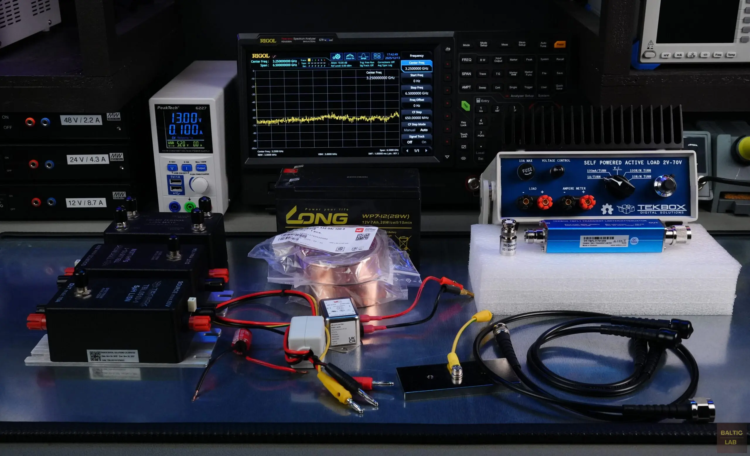
A practical debug process starts with measurement. Use a LISN and spectrum analyzer or EMI receiver for conducted emissions. Use a current probe around line and neutral together to identify common-mode current. If the probe surrounds both conductors and the signal remains, the current is common-mode. If it largely cancels, the problem is more likely differential-mode.
Next, identify the frequency range. Low-frequency peaks near the switching frequency and its early harmonics often need input-current and differential-filter work. Higher-frequency peaks, cable-sensitive peaks, and radiated failures usually point toward common-mode paths.
Then test the source candidates one by one. Adjust gate resistance slightly and watch whether the high-frequency band changes. Add a temporary snubber close to the switch or rectifier. Temporarily bond or isolate a heat sink in a controlled way. Try a temporary transformer shield or compare against a shielded transformer sample if available. Move the Y capacitor return point with short test wiring and see whether the peak follows.
After the source and path are understood, finalize the filter. Select the common-mode choke by impedance in the problem band, rated current, temperature rise, insulation system, and saturation behavior under real line conditions. Select Y capacitors by safety class, working voltage, leakage-current budget, and physical placement. Re-test with the final cable harness and enclosure, because the product-level structure is part of the EMC system.
What buyers should ask from a power supply supplier
For B2B buyers, common-mode noise is not only an engineering nuisance. It affects certification time, machine commissioning, field reliability, and the cost of last-minute shielding. When comparing switching power supplies, ask for more than nominal output power and efficiency.
Useful questions include whether the power supply has been tested for conducted and radiated emissions in a representative enclosure, whether the transformer uses a controlled shielding structure, what leakage current is expected with the Y-capacitor network, and how the supplier controls transformer winding and layout consistency in production. For DIN-rail and open-frame supplies, installation guidance for grounding, cable routing, and cabinet bonding is also valuable.
SIPURUI supports industrial power supply projects where EMC margin, reliability, and production consistency matter as much as the nameplate rating. The right supply is not the one with the largest filter parts; it is the one whose noise source, coupling path, grounding, and filter design have been considered together.
Conclusion
Common-mode noise in switching power supplies usually starts at high dv/dt nodes and escapes through parasitic capacitance. The main source may be the MOSFET drain, transformer interwinding capacitance, diode recovery spike, PCB layout, heat sink, or a combination of these. Once the current reaches a cable or chassis path, it can show up as conducted or radiated EMI.
The durable fix is systematic: reduce switching-node stress, control transformer and layout coupling, provide a defined return path, and then use common-mode chokes and Y capacitors with the right frequency behavior and safety margin. That approach takes more thinking than adding parts at the end, but it is far more likely to pass EMC testing in both prototype and production.
Buyer Checklist
- Use current probing to confirm whether the failing current is common-mode or differential-mode.
- Inspect MOSFET drain copper, transformer interwinding capacitance, secondary rectifier ringing and Y-capacitor routing.
- Check heat-sink bonding, chassis spacing, cable routing and enclosure effects under the final installation conditions.
- Select common-mode chokes by impedance in the failing frequency band, not only by rated current or size.
- Confirm leakage current, safety class, EMC margin and production consistency before release.