When an SMPS fails EMC testing, the next change should come from measured evidence—not a default assumption about PCB layout or filters. Learn how to separate noise modes, identify bypass paths and choose the right corrective action.
Overview
An SMPS fails the emissions scan, so the first bench change is often a larger common-mode choke or another capacitor. Sometimes the peak falls. Sometimes it moves. In the worst case, the new network adds cost, heat or a resonance while the original noise path remains untouched.
The useful question is not whether layout matters more than filtering in general. It is whether the failed measurement is dominated by noise generation, unintended coupling, an inadequate suppression network, or a combination of them. That distinction determines whether the next change belongs in the PCB, the transformer, the filter, the snubber or the installation.
This guide covers conducted and radiated emissions in switching power supplies, with particular attention to isolated industrial AC/DC units. It does not cover immunity failures such as resets during surge, EFT or ESD testing.
Why the layout versus filter shortcut is incomplete
A switching converter produces high dv/dt at switching nodes and high di/dt in commutation loops. Parasitic inductance turns current transitions into voltage spikes. Parasitic capacitance carries displacement current into heatsinks, chassis, secondary circuits and external cables. Those mechanisms can produce differential-mode conducted noise, common-mode conducted noise and radiated fields.
Layout sets the geometry and impedance of these paths. Filters and damping networks change the impedance seen by the noise. The two are coupled: a well-selected capacitor performs poorly when a long connection adds inductance, and a compact hot loop can still fail if transformer capacitance drives common-mode current onto a long output cable.
For many mains-port emissions standards, conducted measurements cover 150 kHz to 30 MHz and radiated measurements begin at 30 MHz. These ranges are useful orientation, not a universal product specification. The applicable standard, port, detector, distance and upper frequency depend on the product and test plan.
Build a repeatable baseline first
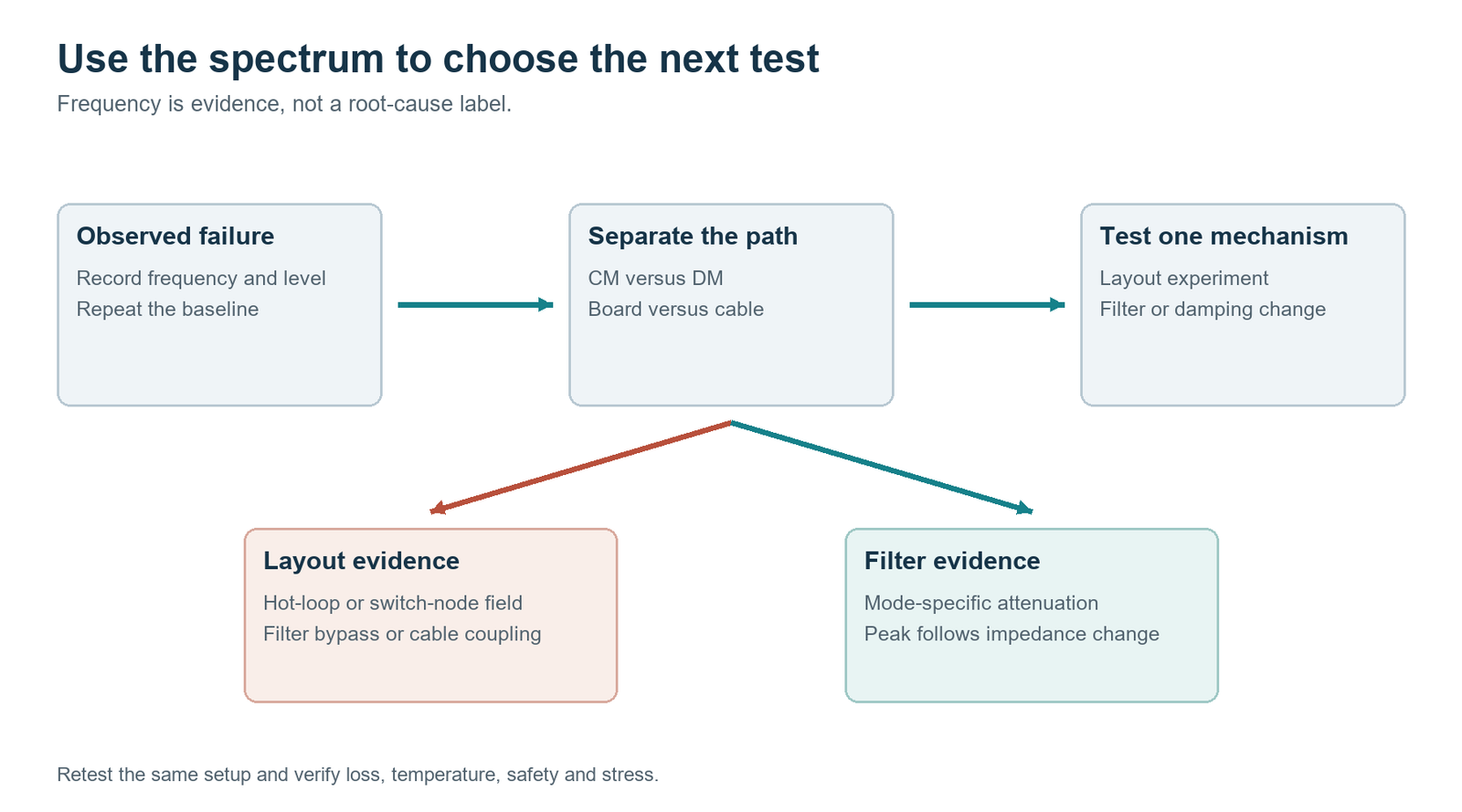
Before changing hardware, record the failed frequency, level, limit line, detector and margin. Photograph the LISN, ground plane, cable routing, enclosure and load connection. Record input voltage, output current, operating mode and thermal state. Repeat the baseline scan without moving the setup.
If the repeated result changes materially, solve the setup or operating-state problem before comparing modifications. Cable position, intermittent bonding, burst mode and load transitions can easily masquerade as an improvement.
The following observations are useful working clues. None is proof on its own.
| Observation | Working hypothesis | Next measurement |
|---|---|---|
| Peaks at the switching frequency and lower harmonics | Input ripple may dominate the differential-mode result | Separate CM and DM noise; inspect the local input-current loop |
| A narrow cluster aligns with drain or rectifier ringing | A parasitic resonance may be exciting the failed band | Compare the switching waveform and near-field response at the same frequency |
| A radiated peak changes when an output cable moves | Cable common-mode current or field coupling is involved | Measure RF current on the cable and scan the nearby source region |
| A larger common-mode choke barely changes the result | Noise may bypass the filter, or the choke has low impedance at that frequency | Check CM/DM mode, impedance curves and physical separation across the filter |
| The noise floor rises across a broad band | Multiple coupling paths or poor return geometry may be active | Map hot loops, switch-node copper, return paths and connector-side coupling |
Frequency alone cannot classify common-mode and differential-mode noise. Similar line and neutral amplitudes are suggestive, but ordinary amplitude plots do not preserve the phase information needed for a firm conclusion. Use a suitable CM/DM separator, current probes or a validated measurement method.

Evidence that points toward a PCB layout problem
The high di dt loop is physically large
Identify the current paths that change state abruptly. In a flyback supply, inspect the primary switching loop and the secondary rectification loop. In a buck converter, focus on the input capacitor, high-side switch, low-side switch or diode, and their return connections.
The relevant loop is the high-frequency path, not the DC path drawn most prominently on the schematic. A bulk electrolytic capacitor several centimetres away may supply average energy while a small local capacitor carries the switching current. Long traces and vias add inductance, increasing ringing and magnetic coupling.
Switch-node copper couples into quiet circuits
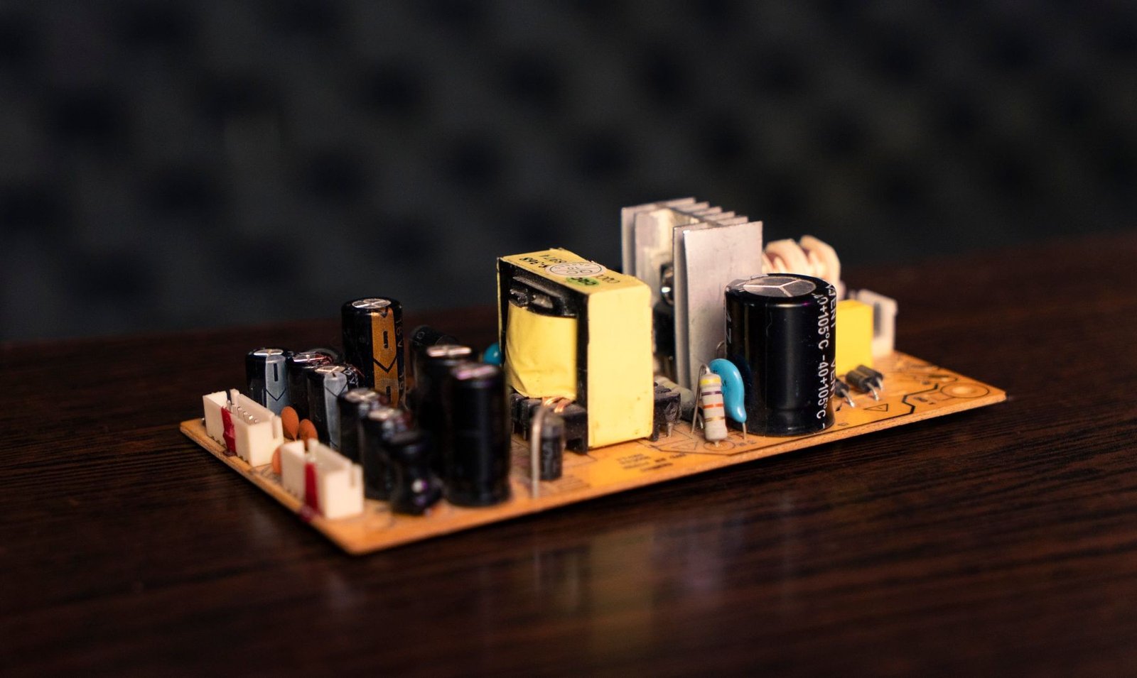
The MOSFET drain, rectifier switching node and transformer winding terminals can have large voltage slew rates. Keep the copper area only as large as current, thermal and creepage requirements demand. Check overlap with feedback routing, current-sense traces, heatsinks and secondary wiring on every layer.
Avoid routing feedback or control traces parallel to high-dv/dt conductors. Use the controller manufacturer's Kelvin and return recommendations. A blanket rule such as splitting every ground plane or joining every ground at one point can make matters worse if it forces a high-frequency return along a longer path.
Noise bypasses the intended filter
An input filter works only when noise must pass through it. Keep the connector side physically separate from the converter side. A trace, transformer, heatsink or cable that couples across this boundary creates a second path around the filter.
Place the mains filter near the entry point where practical. Inspect wiring above the PCB as carefully as copper below it. A harness laid across the choke or transformer can undo the benefit of an otherwise sound schematic.
Ground and chassis paths do not match the design intent
Protective earth, chassis, primary return, secondary return and signal reference serve different functions. Trace the actual high-frequency current paths between them. Narrow shared segments can inject switching current into controller or feedback references. Long chassis connections can have enough inductance to become ineffective at the failed frequency.
Do not treat a copper pour as an equipotential node at RF. Examine where current enters, where it leaves and what lies beneath the path. Return-path continuity usually matters more than an abstract preference for split or solid planes.
The result resists sensible component substitutions
If a properly rated external filter with the correct noise-mode attenuation produces little change, layout or bypass coupling becomes more likely. The same is true when several chokes with suitable impedance curves make almost no difference. This is still not absolute proof: the external filter may be grounded incorrectly, may address the wrong mode or may sit after the coupling point.
| Layout mechanism | Typical bench symptom | Corrective direction |
|---|---|---|
| Large switching-current loop | Broad emissions increase or strong near-field magnetic response around the power stage | Re-place the switching components and local capacitor; shorten outgoing and return paths |
| Excessive switch-node copper | Strong electric-field response and coupling to adjacent traces or heatsinks | Reduce copper area and overlap while preserving thermal and safety margins |
| Filter input and output coupled together | A better filter gives less attenuation than expected | Separate noisy and quiet sides on the PCB and in the harness |
| Shared noisy return with control circuitry | Jitter, control disturbance or a raised noise floor | Re-route high-frequency return current and use required Kelvin connections |
| Cable routed beside the power stage | Radiated peak changes with cable position | Move the cable, reduce coupled common-mode current and control the chassis return |
Evidence that points toward a filter or damping problem
CM and DM separation identifies the missing attenuation
Differential-mode noise flows out on one conductor and returns on the other. Common-mode noise flows in the same direction on the conductors under examination and returns through chassis, earth or parasitic capacitance. The mitigation networks are different, so separate the modes before changing parts.
For differential-mode noise, evaluate the input-current ripple, X capacitor, series inductance, damping and local high-frequency bypassing. For common-mode noise, evaluate common-mode choke impedance, winding capacitance, transformer capacitance, Y-capacitor return paths and cable currents.
The installed component lacks impedance at the failed frequency
Nominal inductance does not describe a choke's complete RF behaviour. Self-resonance, winding capacitance, core loss, bias, current rating and construction matter. Compare impedance curves at the failed frequency rather than selecting only by millihenries.
Capacitors also stop behaving ideally. Connection inductance and dielectric characteristics can limit their high-frequency effect. Adding capacitance can shift a resonance or destabilize an input filter. Check the converter input impedance and provide damping where required.
A controlled snubber change tracks a narrow peak
When a failed peak follows measured drain, switch-node or rectifier ringing, tune an RC or RCD network close to the source. A useful experiment changes one parameter, verifies reduced ringing at the same frequency and then repeats the emissions scan.
Check switch stress, resistor dissipation, efficiency and temperature before accepting the change. A slower switching edge can reduce high-frequency energy but increase switching loss. The passing configuration must remain safe over line, load and temperature.
The Y capacitor return path is valid but insufficient
In an isolated two-wire supply, a safety-approved capacitor between primary and secondary can provide a local common-mode return. It does not have to connect to protective earth, which may not exist. Its connection points, safety class and routing determine the current path.
Increasing Y capacitance may improve emissions while increasing leakage or touch current. Verify the applicable safety requirements for the complete product. An ordinary high-voltage capacitor is not a substitute for the required safety-approved part.
| Network | Evidence that supports changing it | Tradeoff to verify |
|---|---|---|
| Common-mode choke | CM current dominates and candidate impedance is higher at the failed band | Saturation, heating, parasitic capacitance and differential leakage inductance |
| Differential-mode input filter | DM separation shows insufficient attenuation near switching harmonics | Resonance, damping and interaction with converter input impedance |
| Y capacitor | Common-mode current returns through transformer or stray capacitance | Safety class, touch current, leakage current and isolation requirements |
| RC or RCD snubber | Emissions peak tracks a measured switching resonance | Device stress, resistor pulse rating, temperature and efficiency |
| Output ferrite or common-mode choke | Output-cable RF current correlates with the radiated failure | Load current, voltage drop, heating and impedance at frequency |
A practical decision sequence
Start with the failed test configuration and preserve it. Then work through the following sequence.
Repeat the baseline and confirm the failure is stable.
Separate common-mode and differential-mode conducted noise where applicable.
Correlate failed frequencies with switching waveforms, near-field probe response and cable current.
Inspect hot-loop geometry, switch-node area, return paths and coupling across the filter boundary.
Test one reversible change that addresses the suspected mechanism.
Repeat the same scan and record the delta at the failed frequencies.
Verify loss, temperature, safety spacing, touch current and device stress.
Retest the final mechanical build across relevant line, load and cable configurations.
A temporary external filter is useful when it is correctly rated and connected. A clamp ferrite around both output conductors can test common-mode cable current. Moving a cable can expose coupling. A small copper shield connected to the intended reference can be a diagnostic experiment. None of these temporary changes should be mistaken for a production solution without full electrical and safety review.
Why the original seventy percent claim should be removed
There is no defensible universal percentage assigning SMPS EMC failures to PCB layout. Product topology, power level, enclosure, transformer, cables, installation and test standard all change the failure population. Publishing a fixed 70/30 split would create false confidence and encourage engineers to skip measurements that can distinguish the actual path.
A better rule is operational: inspect layout and unintended coupling early because they can limit the performance of every filter added later. Use CM/DM separation and controlled experiments to decide whether the next change belongs in the physical implementation or the suppression network.
Procurement and production implications
For an OEM or automation integrator, a passing test report is useful only when its configuration matches the intended installation. Ask for the tested input voltage, load, enclosure, grounding, cable lengths and external filters. Confirm the PCB and transformer revision represented by the report.
If a corrective action changes the transformer construction, choke, capacitor safety class or PCB, place the change under revision control. Test representative assemblies rather than relying on one hand-tuned prototype. Winding capacitance, lead dress and chassis bonding can vary enough to change high-frequency results.
Choose the next change from measured evidence
PCB layout controls the noise source geometry and the parasitic paths around the suppression network. Filters and snubbers provide targeted attenuation when their installed impedance matches the dominant mode and failed frequency. Treating either category as the default answer wastes chamber time.
SIPURUI can discuss power-supply selection and integration against a customer's target EMC environment. Final compliance still belongs to the complete equipment configuration, including enclosure, wiring, grounding and load.
Buyer Checklist
- Repeat the baseline without moving cables or changing operating state.
- Separate common-mode and differential-mode conducted noise where applicable.
- Correlate failed frequencies with switching waveforms, near-field response and cable current.
- Inspect hot loops, switch-node area, return paths and filter-boundary coupling.
- Retest the final mechanical build across relevant line, load and cable configurations.