Unstable SMPS output can come from feedback sampling, loop compensation, output capacitor behavior, VCC supply, power-stage margin, PCB parasitics, light-load burst mode, or snubber resonance. This guide gives a practical order for finding the cause.
Overview
An unstable output is one of the most common switching power supply problems found during prototype debugging, incoming inspection, and production maintenance. The symptom may look simple on a meter: the output voltage moves, dips, jumps, or refuses to settle. The cause is rarely that simple.
For an overseas equipment builder or industrial buyer, the important question is not "which capacitor should we replace first?" It is "what should we measure first so we do not chase the wrong fault?" A 24 V supply that drifts at no load, collapses during a motor start, or oscillates at light load may need three different fixes.
This guide turns the common Chinese field-service question "when the SMPS output is unstable, what should we check first?" into a practical engineering workflow. It is written for hardware engineers, automation integrators, production technicians, and sourcing teams that need stable output behavior across real input voltage, load, temperature, and wiring conditions.
First, classify the instability
Before touching the BOM, group the symptom. This one step saves a surprising amount of time because each failure pattern points to a different part of the supply.
Static drift appears when the supply is unloaded or running at a steady light load. The output slowly moves up and down, the set voltage is not repeatable, or the unit shows temperature drift. This usually points toward feedback sampling, reference accuracy, optocoupler behavior, leakage paths, or noisy sense routing.
Dynamic instability appears when the static output looks fine, but the voltage overshoots, undershoots, or rings after a load step. This is usually a control-loop and output-filter problem. A DMM may show a healthy average voltage while the oscilloscope shows the real story.
Operating-condition instability happens only at low AC input, high AC input, cold start, full load, high ambient temperature, or long output wiring. This group often involves magnetics margin, MOSFET or rectifier stress, current-limit threshold, auxiliary VCC supply, thermal rise, or load impedance.
Periodic instability has a rhythm. The output may pulse, flicker, or carry a low-frequency envelope. This can come from loop oscillation, burst-mode behavior, repeated start-up attempts, auxiliary supply collapse, or snubber and parasitic resonance.
| Symptom group | Typical field observation | First area to check | Useful first measurement |
|---|---|---|---|
| Static drift | No-load voltage is inaccurate, output wanders, temperature changes the set point | Feedback divider, reference, optocoupler, sense routing | DC output plus feedback/reference node over time |
| Dynamic instability | Voltage droops, overshoots, or rings during load changes | Loop compensation and output capacitor network | Load-step waveform on oscilloscope |
| Condition-specific instability | Fails only at low line, high line, cold start, full load, or hot soak | VCC supply, magnetics, current limit, thermal margin | Input, output, VCC, and switch current under the failing condition |
| Periodic pulsing | Repeating low-frequency output movement or light-load flicker | Loop stability, burst mode, hiccup, snubber resonance | Output waveform with long timebase and trigger holdoff |
Priority 1: feedback sampling and reference accuracy
If the output is wrong or drifting in a steady condition, start with the feedback path. In isolated flyback supplies, this means the output divider, TL431 or reference circuit, optocoupler, compensation parts, and the secondary-side return path. In non-isolated converters, it means the feedback divider, error amplifier input, sense ground, and any remote-sense wiring.
The divider resistors should be checked for value, tolerance, temperature coefficient, solder quality, and contamination around high-impedance nodes. A 5% resistor may pass a low-cost BOM review and still create a loose output tolerance window. More quietly, mismatched temperature coefficients in the upper and lower divider resistors can move the output set point as the board warms up.
Layout matters as much as nominal resistance. A feedback trace routed near a switching node, transformer drain waveform, output rectifier current loop, or noisy ground copper can inject enough disturbance to make the controller correct a problem that is not really present at the load. The result is a wandering or jittery output.
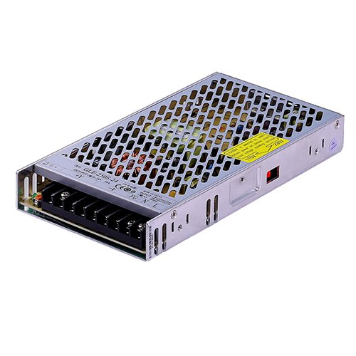
For production troubleshooting, inspect solder joints and connector pressure before changing values. Hairline cracks, flux residue, board contamination, and poor optocoupler soldering can create intermittent feedback behavior. If the output shifts when the board is tapped or warmed locally, the feedback path deserves close inspection.

Priority 2: loop compensation stability
When the output is correct at steady load but badly behaved during load changes, the control loop moves to the top of the list. Many unstable supplies use copied compensation values that never matched the real transformer, output capacitor ESR, switching frequency, control IC mode, or load range.
Loop instability can look like high ripple, poor transient response, audible pulsing, or repeated recovery after every load edge. In a flyback design using TL431 and optocoupler feedback, the optocoupler current transfer ratio, TL431 bias current, compensation capacitor, and output capacitor ESR all shape loop behavior. In buck converters, the modulator, inductor, output capacitor, current-mode slope compensation, and Type-II or Type-III network must be treated as one system.
A good practical target is usually a stable phase margin around 45 to 60 degrees, with enough gain margin to cover component tolerance, temperature, aging, and production spread. The exact target depends on topology and load requirements, but a supply that only behaves on one bench sample has not been designed with enough margin.
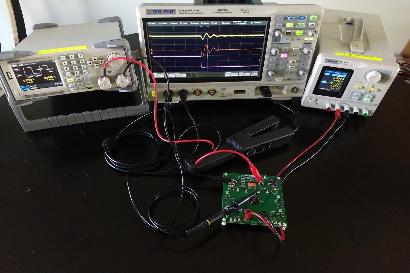
Use a load-step test early. Step the load between realistic current levels and capture output voltage recovery, not just peak-to-peak ripple. Long ringing after a load edge points toward loop compensation or the output capacitor network. A deep dip with clean recovery may point more toward output capacitance, ESR, cable drop, or current limit.
Priority 3: output filter network
Output capacitors are important, but they are not a magic repair. Adding capacitance without understanding the loop can make a marginal supply worse. The right filter network covers energy storage, ripple current, high-frequency impedance, temperature, lifetime, and loop assumptions.
Electrolytic or polymer capacitors provide bulk energy and useful damping. MLCCs provide low ESL and high-frequency current paths, but their real capacitance may drop sharply under DC bias. A design that looks generous on paper can become thin at operating voltage. Aging and ripple current heating add another layer of production risk.
Check the output capacitor bank by function rather than by headline capacitance. Is there enough bulk energy for the expected load step? Is the ESR range compatible with loop stability? Are the capacitors rated for ripple current and temperature? Are the high-frequency capacitors placed close to the rectifier or synchronous switch current loop? Are output cable inductance and load input capacitance part of the same resonance?
| Area | Common mistake | Better engineering check |
|---|---|---|
| Bulk capacitance | Adding a larger electrolytic and assuming the problem is solved | Measure load-step droop and recovery at the actual current slew rate |
| ESR | Replacing electrolytics with very-low-ESR parts without loop review | Verify loop stability across capacitor tolerance and temperature |
| MLCCs | Counting nominal capacitance without DC-bias derating | Check effective capacitance at working voltage |
| Placement | Putting capacitors where they fit mechanically | Keep the first high-frequency output capacitor in the real switching current loop |
| Lifetime | Passing room-temperature tests only | Review ripple current, hot-spot temperature, and expected service life |
Priority 4: VCC supply and start-up behavior
Auxiliary supply problems create some of the most misleading output symptoms. The output may jump at start-up, restart under load, or behave poorly at low temperature. The output stage looks guilty, but the PWM controller is losing stable VCC.
In an isolated flyback supply, the controller often starts through a high-value resistor or start-up source, then runs from an auxiliary winding. If the start-up resistor is too large, the VCC capacitor is too small, the auxiliary winding voltage is marginal, or the auxiliary rectifier has poor behavior, the controller may hit undervoltage lockout during load transitions.
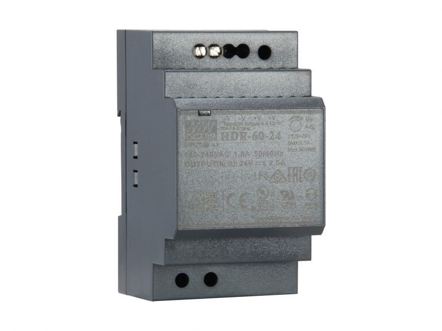
Do not guess here. Put a scope on VCC and capture start-up, load application, low-line full-load operation, and cold start if that is the failure mode. A VCC dip that crosses the UVLO threshold explains repeated pulsing better than another output capacitor swap.
Priority 5: power-stage stress, saturation, and current limit
If the instability appears mainly at full load, low input voltage, or high temperature, check power-stage margin. Transformer saturation, output inductor saturation, MOSFET margin, rectifier heating, current-sense tolerance, and overly conservative current-limit settings can all reduce delivered energy.
At low line, primary current rises to transfer the same power. Magnetics operate closer to saturation, MOSFET conduction loss rises, and current-sense thresholds become more visible. If the supply enters cycle-by-cycle current limit too early, the output may sag or pulse even though nothing is visibly damaged.
For maintenance teams, this is where comparing a failing unit with a known-good unit helps. Capture switch current, drain or switch-node waveform, output voltage, and temperature under the same input and load. A supply that is stable at half load but unstable near nameplate rating may be underdesigned, degraded, or incorrectly derated for its environment.
Priority 6: PCB layout, grounding, and parasitic coupling
A schematic can be correct while the board is unstable. Feedback traces, signal ground, power ground, transformer secondary loops, rectifier current loops, and output return paths all carry physical behavior that the simplified drawing hides.
Ground bounce is a common example. If high di/dt current flows through copper that is also used as the feedback reference, the controller sees a moving ground. It then adjusts duty cycle based on a false feedback signal. The output appears unstable even though every part value checks correctly.
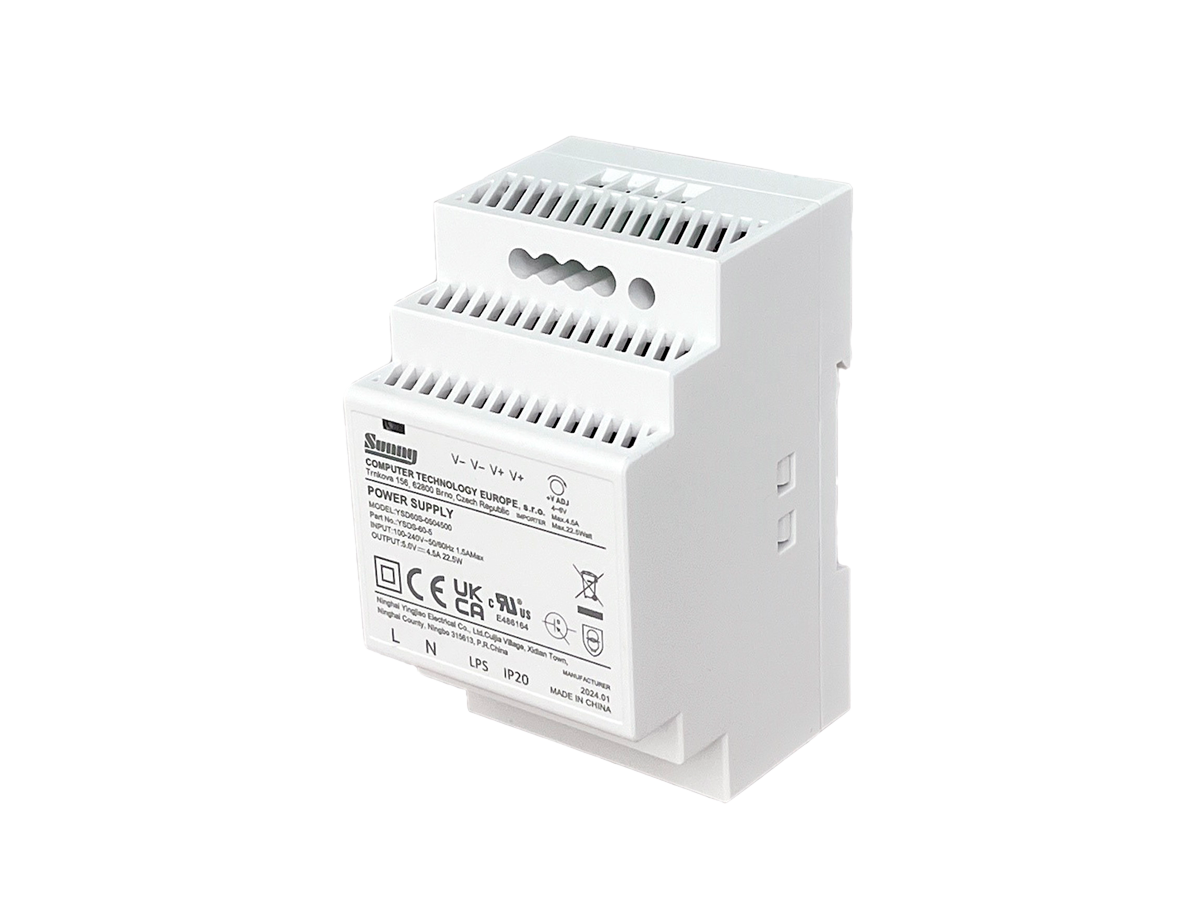
Keep feedback routing short, quiet, and away from switch nodes. Separate power current paths from small-signal sensing. Use a clean return point for the feedback divider and optocoupler reference. In high-current supplies, review copper thickness, via count, and connector placement as part of the stability investigation.
Priority 7: light-load burst mode and intermittent operation
Many modern controllers improve standby efficiency by skipping pulses, entering burst mode, or reducing switching frequency at light load. That is normal behavior, but it can become a problem when the end product requires clean no-load or light-load output.
Typical symptoms include no-load voltage flicker, low-frequency output ripple, audible ticking, or repeated small output corrections. The supply may be excellent at 50% load and poor at 2% load. For PLC input modules, sensors, analog circuits, audio equipment, or precision measurement devices, light-load behavior can matter more than full-load efficiency.
If light-load stability is the priority, evaluate the controller mode settings, preload requirement, minimum load specification, and compensation behavior in burst mode. Sometimes a small preload, different compensation value, or disabled burst mode is the correct tradeoff. The efficiency penalty may be smaller than the cost of field complaints.
Priority 8: snubber, clamp, and high-frequency resonance
RCD clamps, RC snubbers, TVS devices, and damping networks protect the switching waveform and reduce high-frequency ringing. Poorly matched values can leave too much spike energy, create heat, or excite parasitic resonance. The output symptom may be high-frequency jitter, intermittent EMI problems, or apparent output movement caused by measurement coupling.
Probe carefully. A long oscilloscope ground lead can invent ringing that is not really present, while a poor probe setup can hide actual spikes. Use short ground connections, appropriate differential or isolated probing where required, and safe high-voltage practice. Then tune the snubber or clamp based on measured waveform, device stress, temperature, and EMI behavior.
A practical troubleshooting order
The best sequence is to move from low-risk signal checks toward higher-energy power-stage checks. Start where the supply decides what the output should be, then move toward the parts that deliver the energy.
| Priority | Check point | Typical unstable output symptom | Practical action |
|---|---|---|---|
| 1 | Feedback sampling path | Wrong set voltage, slow drift, temperature drift, output stuck high or low | Check divider tolerance, reference voltage, optocoupler, soldering, and sense routing |
| 2 | Loop compensation | Load-step ringing, overshoot, periodic envelope, light-load oscillation | Run load-step test, review Type-II/Type-III network, verify phase and gain margin |
| 3 | Output filter | Heavy-load droop, high ripple, poor transient response | Review ESR/ESL, ripple current, capacitor aging, MLCC DC bias, and placement |
| 4 | VCC and start-up | Start-up pulsing, repeated restart, low-temperature failure | Scope VCC during start-up and load application; adjust VCC capacitance or auxiliary supply |
| 5 | Power-stage margin | Full-load instability, low-line sag, heating-related droop | Check magnetics saturation, MOSFET/rectifier stress, current limit, and derating |
| 6 | PCB layout and grounding | Unit-to-unit variation, touch-sensitive behavior, unexplained jitter | Separate power and signal returns, shorten feedback routing, reduce loop area |
| 7 | Light-load mode | No-load flicker, low-frequency pulsing, standby ticking | Review burst-mode threshold, minimum load, preload, and light-load compensation |
| 8 | Snubber and resonance | High-frequency spikes, EMI-related output disturbance | Tune clamp/snubber values from measured waveforms, not from guesswork |
Mistakes that slow down the repair
The first mistake is replacing the output capacitor bank before the symptom is classified. Capacitors are easy to change, so they get blamed. If the root cause is feedback noise or a VCC collapse, the repair will not hold.
The second mistake is measuring only the output with a multimeter. A meter is useful for set voltage, but it hides ripple envelopes, start-up dips, recovery ringing, and burst packets. Output instability is a waveform problem as much as a DC-value problem.
The third mistake is copying compensation values from a reference design without validating the actual transformer, optocoupler, capacitor ESR, PCB layout, and load. Reference designs are starting points, not proof of production stability.
The fourth mistake is testing only at room temperature and nominal line. Many supplies fail at cold start, low AC input, high ambient temperature, or with the real load attached. A proper troubleshooting routine reproduces the customer's condition, not the easiest bench condition.
Buyer and production checklist
For B2B buyers, output stability should be part of supplier evaluation. Ask for more than rated voltage and current. Stable output over input range, load range, temperature, and production tolerance is what protects the downstream machine.
| Evaluation item | What to request from a supplier | Why it matters |
|---|---|---|
| Load-step data | Output droop, overshoot, recovery time, and test current levels | Shows real dynamic regulation |
| Ripple and noise method | Probe method, bandwidth limit, cable length, and load condition | Prevents misleading numbers |
| Low-line and full-load test | Stable operation at minimum input and rated load | Exposes transformer, MOSFET, and current-limit margin |
| Cold-start behavior | Start-up waveform at low ambient temperature | Finds VCC and capacitor weaknesses |
| Capacitor and thermal margin | Capacitor series, ripple rating, temperature rise, expected life | Reduces field failures from aging |
| Layout and grounding review | Feedback routing, power loop area, signal-ground treatment | Explains consistency across batches |
Conclusion
Unstable SMPS output is not a single-component fault. It is usually the visible result of feedback accuracy, loop stability, output filter behavior, auxiliary supply margin, power-stage stress, PCB parasitics, light-load mode, or resonance.
The most reliable order is simple: classify the symptom, inspect feedback and reference behavior, test the loop dynamically, review the output filter, capture VCC, then move into magnetics, current limit, layout, burst mode, and snubber details. That order prevents unnecessary BOM changes and shortens the path from symptom to cause.
For industrial control cabinets, automation equipment, LED systems, and OEM machines, stable output is a reliability feature, not a cosmetic specification. SIPURUI can support switching power supply selection where output regulation, practical derating, and production consistency need to match real operating conditions rather than only nameplate ratings.
Buyer Checklist
- Classify the instability pattern before replacing capacitors or power parts.
- Measure feedback, reference, output waveform, and VCC behavior under the failing condition.
- Run realistic load-step tests instead of relying only on a steady multimeter reading.
- Review output capacitor ESR, ripple current, DC-bias derating, placement, and service temperature.
- Ask suppliers for load-step data, ripple test method, low-line full-load testing, cold-start behavior, and capacitor thermal margin.