Excessive output ripple is rarely solved by adding the biggest capacitor that fits. This bench-ready guide shows how to identify the waveform mechanism, correct the measurement, and apply the right circuit or layout fix.
Overview
Excessive output ripple is rarely solved by adding the biggest capacitor that fits. That approach sometimes lowers the periodic ripple, but it can leave switching spikes unchanged, destabilize the control loop, or move the problem into higher capacitor current and temperature.
The faster route is to identify what the oscilloscope is actually showing. A power supply output may contain switching-frequency ripple, edge-related spikes, low-frequency burst-mode variation, ground bounce, and measurement pickup at the same time. Each component has a different source and calls for a different fix.
This guide presents a bench-ready method for engineers, equipment manufacturers, and power supply buyers. It starts with measurement because a bad probe connection can make a sound converter look defective.
Start by separating ripple from noise
“Ripple and noise” is often specified as one peak-to-peak number, but the waveform usually contains several mechanisms.
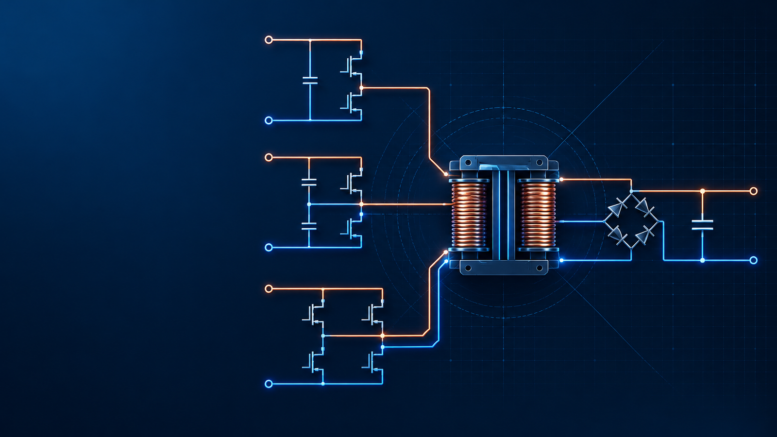
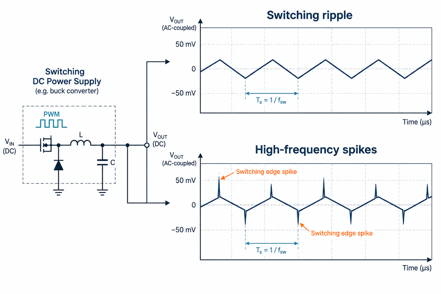
Switching ripple is the repetitive component related to the converter switching cycle. In a buck converter, inductor ripple current flows into and out of the output capacitor. In an isolated flyback supply, the secondary rectifier charges the capacitor during part of the cycle while the capacitor supports the load during the rest. The resulting waveform often appears triangular or sawtooth-like.
High-frequency noise appears as narrow spikes or damped ringing around switching transitions. It is driven by fast di/dt and dv/dt, rectifier reverse recovery, leakage inductance, capacitor ESL, and PCB loop inductance. Its frequency may be tens or hundreds of megahertz even when the converter switches at a few hundred kilohertz.
Low-frequency modulation is another category. Burst mode, pulse skipping, hiccup behavior, input ripple, or an unstable control loop can create an envelope from a few hertz to several kilohertz. Treating this as ordinary switching ripple leads engineers toward the wrong components.
| Waveform signature | Likely mechanism | First checks |
|---|---|---|
| Regular triangular or sawtooth waveform at the switching frequency | Inductor/capacitor charge balance; output capacitor impedance | Capacitance under bias, ESR at operating frequency, inductor ripple current |
| Narrow spikes aligned with switch edges | Parasitic inductance, rectifier recovery, transformer coupling, probe pickup | Probe loop, hot-loop layout, rectifier waveform, snubber |
| Ripple increases steadily with load | Higher ripple current, capacitor ESR heating, excessive secondary-path impedance | Capacitor RMS rating, connector and trace resistance, rectifier current |
| Large ripple at light load but lower ripple at moderate load | Burst mode or pulse skipping | Controller operating mode, minimum load, light-load settings |
| Slow oscillation or repeating envelope | Loop instability, input modulation, protection cycling | Load-step response, compensation, input rail, optocoupler operating point |
| Waveform changes when the probe or hand moves | Measurement pickup or grounding problem | Ground spring, coax connection, probe placement, ground loop |
Fix the measurement before changing the circuit
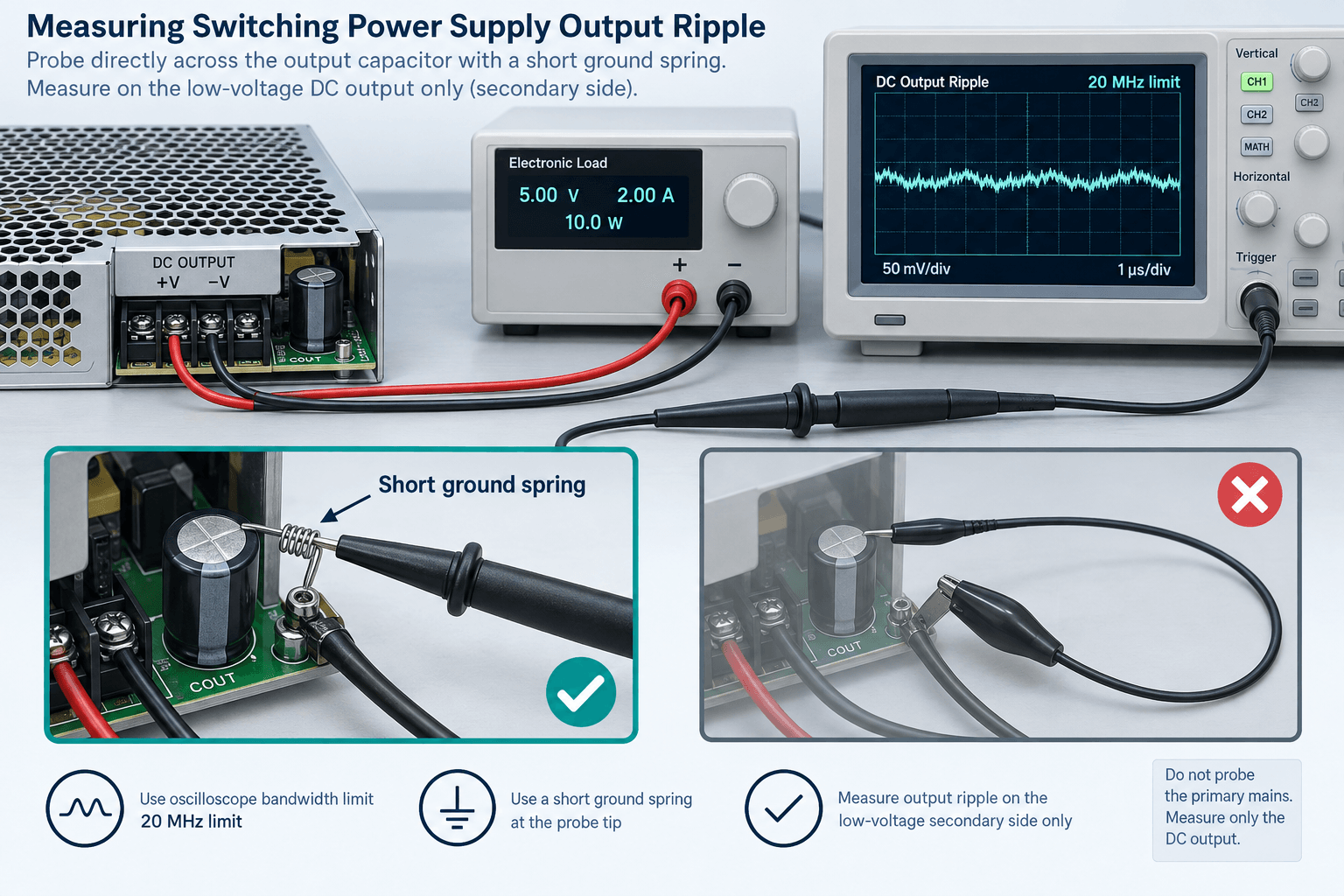
An oscilloscope probe with a long ground lead forms an antenna and a high-inductance loop. It readily picks up the converter's switching magnetic field. The displayed spikes may therefore come from the probing arrangement rather than the output terminals.
Use the shortest ground connection available, preferably a probe ground spring or a coaxial tip-and-barrel adapter. Measure directly across the output capacitor or at the specified output connector, not at a convenient ground point several centimeters away. Enable the oscilloscope's 20 MHz bandwidth limit when the product specification calls for it, and document whether the measurement is AC-coupled or DC-coupled. A measurement made with full instrument bandwidth is valid too, but it answers a different question and will usually report more high-frequency energy.
Also record the operating conditions: input voltage, output load, ambient temperature, warm-up time, probe point, bandwidth, and time scale. A ripple number without these conditions is not repeatable enough for supplier qualification.

What sets the ripple amplitude
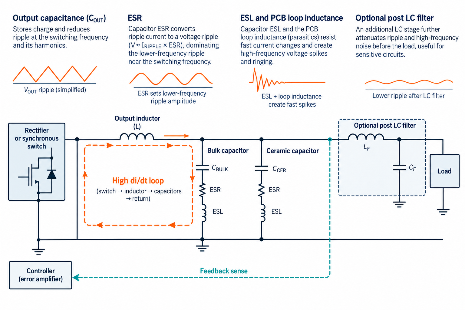
The capacitor is not an ideal capacitance. Its impedance includes capacitance, equivalent series resistance (ESR), and equivalent series inductance (ESL). A useful engineering approximation is:
V ripple ≈ ΔI × ESR + ΔQ / C + ESL × di/dt
The terms dominate in different frequency regions. Capacitance controls the charge-related component, ESR converts ripple current into a voltage step, and ESL becomes important at fast switching edges. PCB trace and via inductance add to the component's own ESL.
This is why a larger aluminum electrolytic capacitor may make little difference to a narrow spike. It adds useful energy storage but may have too much impedance at the spike frequency. Conversely, a small ceramic capacitor can shunt high-frequency current well but cannot supply a long load transient by itself.
DC bias must be included when evaluating multilayer ceramic capacitors. A nominal 22 µF MLCC can lose a substantial share of its capacitance near its rated voltage, depending on case size, dielectric, and manufacturer. Use the vendor's bias curve rather than the label value.
| Capacitor technology | Strength | Limitation | Best use in a ripple network |
|---|---|---|---|
| Aluminum electrolytic | High bulk capacitance at low cost | Higher ESR and ESL; lifetime depends on temperature and ripple current | Energy storage and lower-frequency ripple |
| Polymer capacitor | Low ESR and high ripple-current capability | Higher cost; fewer high-voltage options | Low-ripple, medium- to high-current outputs |
| MLCC | Very low ESR/ESL and fast response | DC-bias derating; possible acoustic effects; can reduce loop damping | High-frequency decoupling placed at the current loop |
| Tantalum | Compact with stable capacitance | Surge and inrush sensitivity; requires voltage derating | Controlled low-power rails where surge conditions are known |
A mixed network is usually effective: bulk electrolytic or polymer capacitance for energy storage, plus one or more ceramics close to the rectifier and return path. Do not copy a generic “1000 µF + 10 µF + 0.1 µF” stack without checking impedance. Parallel values can create anti-resonance peaks. An impedance analyzer or a vendor simulation tool reveals whether the network is actually low impedance across the required band.
Stop switching spikes at their source
If the main problem is an edge-aligned spike, adding bulk capacitance at the output is usually inefficient. Inspect the switching node and rectifier current path instead.
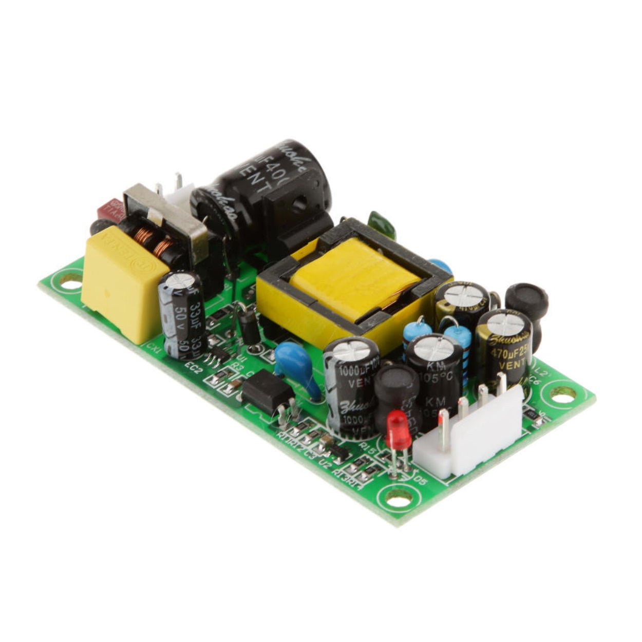
In a flyback converter, secondary rectifier reverse recovery and transformer leakage inductance can form a ringing network. Schottky, ultrafast, or SiC rectifiers may reduce recovery charge, but the correct choice depends on voltage, current, leakage, temperature, and cost. Synchronous rectification has its own timing and common-source-inductance concerns.
An RC snubber across a rectifier or switching node can damp ringing. Select it from the measured ringing frequency and impedance, then verify dissipation and efficiency at line and load extremes. Increasing the snubber capacitor until the trace looks clean is not a design method; it may simply turn switching energy into heat.
For flyback primary leakage spikes, an RCD clamp, active clamp, or other clamp network protects the MOSFET and can reduce coupled noise. The clamp must be evaluated with the actual transformer leakage inductance. Transformer construction, interwinding capacitance, shielding, and winding order can matter as much as the schematic.
Use a post-filter carefully
A second-stage LC or ferrite-bead filter can provide substantial attenuation when the required output ripple is only a few millivolts. It is often more effective than forcing the main output capacitor bank to do everything.
The filter is not electrically invisible. Its resonance can peak, reduce damping, and interact with the converter output impedance or remote load. Keep the filter corner well below the switching frequency, but do not rely on that rule alone. Add damping where needed, check the control-loop response at the correct sensing point, and run load-step tests across the full input and load range. If the converter senses before the post-filter, load regulation after the filter also deserves attention.
Ferrite beads help with high-frequency noise but can saturate under DC current and become resistive. Check the impedance curve at the noise frequency and the current-dependent behavior, not just the “600 Ω at 100 MHz” headline value.
Verify loop stability rather than guessing at compensation
The control loop governs output regulation and load-transient recovery, but it normally does not cancel ripple at the switching frequency. The crossover frequency is typically well below the switching frequency so that the averaged power stage model remains valid. Increasing bandwidth blindly can reduce phase margin and produce oscillation.
Suspect the loop when the waveform has a low-frequency envelope, ringing after a load step, slow recovery, or a response that changes sharply with input voltage or load. For an optocoupler-regulated isolated supply, check TL431 bias, optocoupler current-transfer ratio over temperature and lifetime, and whether the optocoupler is being driven into saturation.
Measure the loop gain with a frequency-response analyzer when possible. Otherwise, a controlled load step is a useful screening test. A monotonic recovery or a small, quickly decaying ring is usually healthier than sustained ringing, although the final judgment must be tied to the converter model and specification. Do not change the compensation network without rechecking current limit, start-up, no-load behavior, and transient response.
PCB layout determines how much of the design survives reality
The most effective ceramic capacitor is the one placed inside the correct high-current loop. Long traces and shared vias add inductance, so a capacitor a few centimeters away may contribute little at the frequency of interest.
Keep the rectifier, output capacitor, and transformer secondary loop compact. On a buck converter, minimize both the input hot loop and the switching-node copper area. Route the feedback divider as a quiet Kelvin connection from the regulated output and return. Do not allow rectifier or MOSFET current to flow through the feedback ground path.
Keep the switch node away from feedback traces, optocoupler networks, current-sense lines, and connector pins that leave the board. A ground plane helps, but it does not repair an undefined current-return path. Placement comes first; routing follows the current loops.
Common topology-specific failure modes
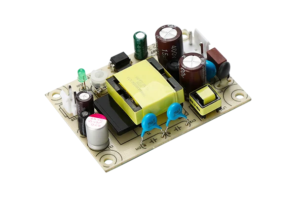
Flyback supplies often show secondary-rectifier ringing, primary leakage-spike coupling, and burst-mode ripple at light load. Transformer construction and the primary clamp deserve early attention.
Buck converters are highly sensitive to hot-loop placement, switch-node coupling, and feedback routing. In synchronous designs, dead time and MOSFET common-source inductance can create sharp edge noise.
Forward converters depend on a well-designed output LC stage and a controlled reset path. Poor damping or compensation can turn a filter improvement into a transient-response problem.
LLC converters benefit from soft switching over their intended range, but they are not automatically quiet. Operation outside the designed gain and load region, rectifier commutation, transformer capacitance, and output-capacitor ESR can still raise ripple and common-mode noise.
A disciplined troubleshooting sequence
Use this order to avoid tuning around a false symptom:
Define the acceptance test. State the measurement point, load, input range, bandwidth, coupling, temperature, and peak-to-peak or RMS limit.
Repeat the measurement with a ground spring or coax adapter. Confirm that the probe loop is not the dominant antenna.
Correlate the output waveform with the switching node. Separate switching-period ripple from edge spikes and low-frequency modulation.
Scan the load range. Test no load or minimum load, then 25%, 50%, 75%, and 100% load. Include dynamic load steps.
Change one mechanism at a time. Try a known low-ESR capacitor, a temporary ceramic placed directly at the loop, or a calculated snubber. Avoid changing capacitance, snubber, and compensation together.
Check temperature and loss. A quieter waveform is not an acceptable fix if it overheats the snubber, rectifier, inductor, or capacitor.
Verify loop stability and protection behavior. Recheck start-up, short circuit, current limit, line transients, and light-load mode after the modification.
Repeat the defined acceptance test. Record the final waveform and component changes so production and suppliers can reproduce the result.
| If the waveform shows... | Try first | Confirm before release |
|---|---|---|
| Switching-frequency ripple | Check effective C, ESR, inductor ripple, and capacitor placement | Capacitor temperature, load transient, stability |
| Edge spikes or ringing | Correct probing, reduce loop area, evaluate rectifier and snubber | MOSFET/diode stress, snubber loss, EMC |
| Light-load burst envelope | Review controller mode and minimum-load requirement | Standby power, audible noise, no-load regulation |
| Low-frequency oscillation | Measure loop response and inspect feedback path | Phase margin, gain margin, line/load corners |
| Ripple copied from the input | Check input capacitor, EMI filter damping, transformer coupling | Hold-up, conducted emissions, inrush |
Define the acceptance test. State the measurement point, load, input range, bandwidth, coupling, temperature, and peak-to-peak or RMS limit.
Repeat the measurement with a ground spring or coax adapter. Confirm that the probe loop is not the dominant antenna.
Correlate the output waveform with the switching node. Separate switching-period ripple from edge spikes and low-frequency modulation.
Scan the load range. Test no load or minimum load, then 25%, 50%, 75%, and 100% load. Include dynamic load steps.
Change one mechanism at a time. Try a known low-ESR capacitor, a temporary ceramic placed directly at the loop, or a calculated snubber. Avoid changing capacitance, snubber, and compensation together.
Check temperature and loss. A quieter waveform is not an acceptable fix if it overheats the snubber, rectifier, inductor, or capacitor.
Verify loop stability and protection behavior. Recheck start-up, short circuit, current limit, line transients, and light-load mode after the modification.
Repeat the defined acceptance test. Record the final waveform and component changes so production and suppliers can reproduce the result.
What power supply buyers should request from a supplier
A single catalog ripple value is not enough for sensitive industrial equipment. Ask for the measurement method, scope bandwidth, probe arrangement, input voltage, output load, and test location. For custom or critical supplies, request waveforms at minimum and maximum load, a load-step result, and confirmation that the quoted limit applies after warm-up.
Also review the capacitor series and temperature rating, not only capacitance. The ripple performance of a prototype with premium capacitors may not represent a production unit after an approved vendor substitution. Component-change control is therefore part of ripple control.
Conclusion
The quickest way to reduce switching power supply ripple is to stop treating every trace as a capacitor problem. First prove the measurement. Then identify whether the dominant component is charge ripple, ESR drop, edge-related ringing, light-load modulation, input feedthrough, or loop instability.
Capacitor impedance, snubber design, loop stability, and PCB current paths must support one another. A fix that lowers the oscilloscope number while raising loss or weakening phase margin is not finished engineering.
For industrial equipment that needs a defined ripple limit across line, load, and temperature, SIPURUI can support power supply selection and application review based on the actual operating conditions rather than a nominal datasheet point.